NCV500(2015) 데이터 시트보기 (PDF) - ON Semiconductor
부품명
상세내역
제조사
NCV500 Datasheet PDF : 18 Pages
| |||
NCP500, NCV500
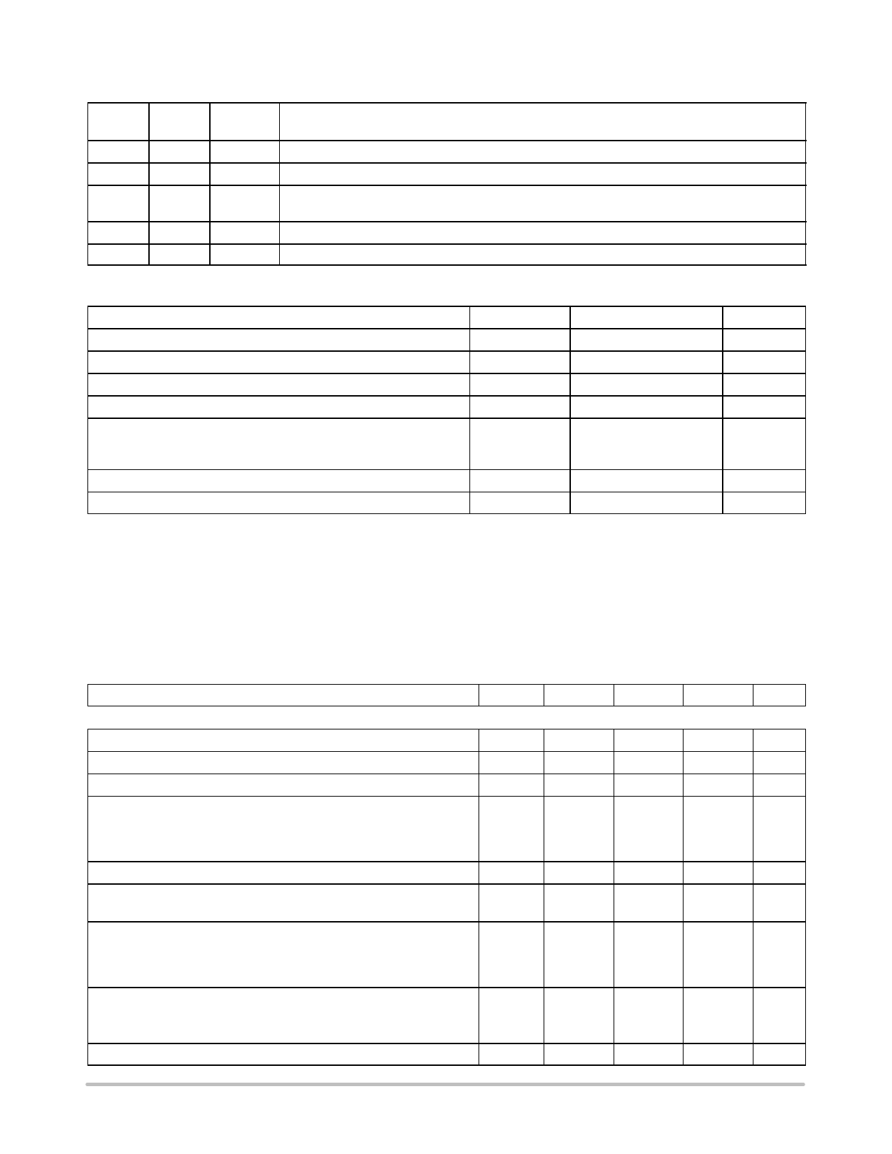
ÁÁÁÁÁÁÁÁÁÁÁÁÁÁÁÁÁÁÁÁÁÁÁÁÁÁÁÁÁÁÁÁÁ PIN FUNCTION DESCRIPTION
ÁÁÁÁÁÁÁÁÁÁÁÁÁÁÁÁÁÁÁÁÁÁÁÁÁÁÁÁÁÁÁÁÁ TSOP−5 DFN2x2
ÁÁÁÁÁÁÁÁÁÁÁÁÁÁÁÁÁÁÁÁÁÁÁÁÁÁÁÁÁÁÁÁÁ PinNo. PinNo. PinName
Description
ÁÁÁÁÁÁÁÁÁÁÁÁÁÁÁÁÁÁÁÁÁÁÁÁÁÁÁÁÁÁÁÁÁ 1
3
Vin
Positive power supply input voltage.
ÁÁÁÁÁÁÁÁÁÁÁÁÁÁÁÁÁÁÁÁÁÁÁÁÁÁÁÁÁÁÁÁÁ 2
2, 5
GND Power supply ground.
ÁÁÁÁÁÁÁÁÁÁÁÁÁÁÁÁÁÁÁÁÁÁÁÁÁÁÁÁÁÁÁÁÁ 3
1
Enable This input is used to place the device into low−power standby. When this input is pulled to a logic
low, the device is disabled. If this function is not used, Enable should be connected to Vin.
ÁÁÁÁÁÁÁÁÁÁÁÁÁÁÁÁÁÁÁÁÁÁÁÁÁÁÁÁÁÁÁÁÁ 4
6
N/C
No internal connection.
ÁÁÁÁÁÁÁÁÁÁÁÁÁÁÁÁÁÁÁÁÁÁÁÁÁÁÁÁÁÁÁÁÁÁÁÁÁÁÁÁÁÁÁÁÁÁÁÁÁÁÁÁÁÁÁÁÁÁÁÁÁÁÁÁÁÁ 5
4
Vout
Regulated output voltage.
MAXIMUM RATINGS
Rating
ÁÁÁÁÁÁÁÁÁÁÁÁÁÁÁÁÁÁÁÁÁÁÁÁÁÁÁÁÁÁÁÁÁ Input Voltage
ÁÁÁÁÁÁÁÁÁÁÁÁÁÁÁÁÁÁÁÁÁÁÁÁÁÁÁÁÁÁÁÁÁ Enable Voltage
ÁÁÁÁÁÁÁÁÁÁÁÁÁÁÁÁÁÁÁÁÁÁÁÁÁÁÁÁÁÁÁÁÁ Output Voltage
ÁÁÁÁÁÁÁÁÁÁÁÁÁÁÁÁÁÁÁÁÁÁÁÁÁÁÁÁÁÁÁÁÁÁÁÁÁÁÁÁÁÁÁÁÁÁÁÁÁÁÁÁÁÁÁÁÁÁÁÁÁÁÁÁÁÁ Output Short Circuit Duration
Symbol
Vin
Von/off
Vout
−
Value
0 to 6.0
−0.3 to Vin +0.3
−0.3 to Vin +0.3
Infinite
Unit
V
V
V
−
Thermal Resistance, Junction−to−Ambient
RqJA
°C/W
TSOP−5
DFN (Note 3)
ÁÁÁÁÁÁÁÁÁÁÁÁÁÁÁÁÁÁÁÁÁÁÁÁÁÁÁÁÁÁÁÁÁ Operating Junction Temperature
ÁÁÁÁÁÁÁÁÁÁÁÁÁÁÁÁÁÁÁÁÁÁÁÁÁÁÁÁÁÁÁÁÁÁÁÁÁÁÁÁÁÁÁÁÁÁÁÁÁÁÁÁÁÁÁÁÁÁÁÁÁÁÁÁÁÁ Storage Temperature
250
225
TJ
+125
°C
Tstg
−65 to +150
°C
Stresses exceeding those listed in the Maximum Ratings table may damage the device. If any of these limits are exceeded, device functionality
should not be assumed, damage may occur and reliability may be affected.
1. This device series contains ESD protection and exceeds the following tests:
Human Body Model 2000 V per MIL−STD−883, Method 3015
Machine Model Method 200 V
Latch up capability (85°C) "100 mA.
2. Device is internally limited to 160°C by thermal shutdown.
3. For more information, refer to application note, AND8080/D.
ELECTRICAL CHARACTERISTICS (Vin = 2.35 V, Cin = 1.0 mF, Cout = 1.0 mF, for typical value TA = 25°C, for min and
max values TA = −40°C to 85°C, Tjmax = 125°C, unless otherwise noted)
Characteristic
Symbol
Min
Typ
Max
−1.8 V
Output Voltage (TA = −40°C to 85°C, Iout = 1.0 mA to 150 mA)
Line Regulation (Vin = 2.3 V to 6.0 V, Iout = 1.0 mA)
Load Regulation (Iout = 1.0 mA to 150 mA)
Dropout Voltage (Measured at Vout −2.0%, TA = −40°C to 85°C)
(Iout = 1.0 mA)
(Iout = 75 mA)
(Iout = 150 mA)
Vout
1.755
1.8
1.845
Regline
−
1.0
10
Regload
−
15
45
Vin−Vout
−
−
−
2.0
10
140
200
270
350
Output Short Circuit Current
Ripple Rejection
(Vin = Vout (nom.) + 1.0 V + 0.5 Vpp, f = 1.0 kHz, Io = 60 mA)
Quiescent Current
(Enable Input = 0 V)
(Enable Input = 0.9 V, Iout = 1.0 mA)
(Enable Input = 0.9 V, Iout = 150 mA)
Enable Input Threshold Voltage
(Voltage Increasing, Output Turns On, Logic High)
(Voltage Decreasing, Output Turns Off, Logic Low)
Iout(max)
200
RR
−
IQ
−
−
−
Vth(EN)
0.9
−
540
62
0.01
175
175
−
−
700
−
1.0
300
300
−
0.15
Enable Input Bias Current
Output Turn On Time (Enable Input = 0 V to Vin)
IIB(EN)
−
−
−
3.0
100
20
100
Unit
V
mV
mV
mV
mA
dB
mA
V
nA
ms
www.onsemi.com
2
Share Link: 