EL5410 데이터 시트보기 (PDF) - Renesas Electronics
부품명
상세내역
제조사
EL5410 Datasheet PDF : 16 Pages
| |||
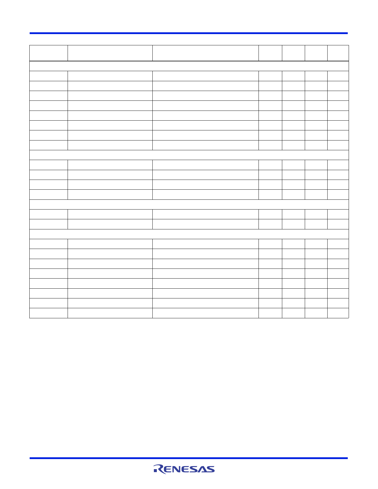
EL5210, EL5410
Electrical Specifications VS+ = 15V, VS- = 0V, RL = 1k and CL = 12pF to 7.5V, TA = +25°C unless otherwise specified.
PARAMETER
DESCRIPTION
CONDITION
MIN
MAX
(Note 4) TYP (Note 4)
UNIT
INPUT CHARACTERISTICS
VOS
TCVOS
IB
RIN
CIN
CMIR
Input Offset Voltage
VCM = 7.5V
Average Offset Voltage Drift (Note 1)
Input Bias Current
Input Impedance
VCM = 7.5V
Input Capacitance
Common-Mode Input Range
3
15
mV
7
µV/°C
2
60
nA
1
GW
2
pF
-0.5
+15.5
V
CMRR
Common-Mode Rejection Ratio
AVOL
Open-Loop Gain
OUTPUT CHARACTERISTICS
for VIN from -0.5V to 15.5V
0.5V VOUT 14.5V
53
72
dB
65
80
dB
VOL
Output Swing Low
VOH
Output Swing High
ISC
Short Circuit Current
IOUT
Output Current
POWER SUPPLY PERFORMANCE
IL = -7.5mA
IL = 7.5mA
170
350
mV
14.65 14.83
V
±120
mA
±30
mA
PSRR
Power Supply Rejection Ratio
IS
Supply Current (Per Amplifier)
DYNAMIC PERFORMANCE
VS is moved from 4.5V to 15.5V
No Load
60
80
dB
2.5
3.75
mA
SR
Slew Rate (Note 2)
1V VOUT 14V, 20% to 80%
tS
Settling to +0.1% (AV = +1)
(AV = +1), VO = 2V Step
BW
-3dB Bandwidth
33
V/µs
140
ns
30
MHz
GBWP
Gain-Bandwidth Product
20
MHz
PM
Phase Margin
50
°
CS
Channel Separation
f = 5MHz
110
dB
dG
Differential Gain (Note 3)
RF = RG = 1k and VOUT = 1.4V
0.10
%
dP
Differential Phase (Note 3)
RF = RG = 1k and VOUT = 1.4V
0.11
°
NOTES:
1. Measured over operating temperature range
2. Slew rate is measured on rising and falling edges
3. NTSC signal generator used
4. Parts are 100% tested at +25°C. Over temperature limits established by characterization and are not production tested.
FN7185 Rev 3.00
July 5, 2007
Page 5 of 16
Share Link: 