IDT74FCT573CTSO 데이터 시트보기 (PDF) - Integrated Device Technology
부품명
상세내역
제조사
IDT74FCT573CTSO Datasheet PDF : 8 Pages
| |||
IDT54/74FCT373T/AT/CT/DT - 2373T/AT/CT, IDT54/74FCT533T/AT/CT, IDT54/74FCT573T/AT/CT/DT - 2573T/AT/CT
FAST CMOS OCTAL TRANSPARENT LATCHES
MILITARY AND COMMERCIAL TEMPERATURE RANGES
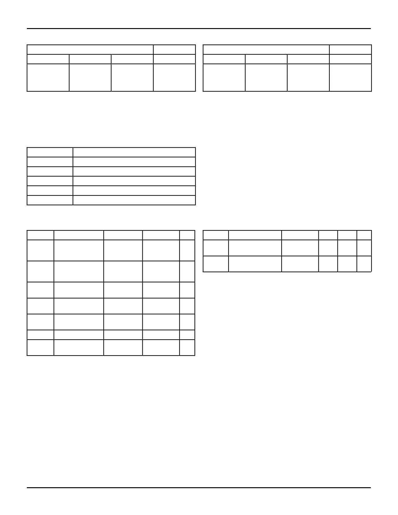
FUNCTION TABLE (533)(1)
Inputs
DN
LE
OE
H
H
L
L
H
L
X
X
H
NOTE:
1. H = HIGH Voltage Level
L = LOW Voltage Level
X = Don’t Care
Z = High Impedance
FUNCTION TABLE (373 and 573)(1)
Outputs
ON
Inputs
DN
LE
OE
L
H
H
L
H
L
H
L
Z
X
X
H
2564 tbl 01
NOTE:
1. H = HIGH Voltage Level
L = LOW Voltage Level
X = Don’t Care
Z = High Impedance
Outputs
ON
H
L
Z
2564 tbl 02
DEFINITION OF FUNCTIONAL TERMS
Pin Names
DN
LE
OE
Data Inputs
Description
Latch Enable Input (Active HIGH)
Output Enable Input (Active LOW)
ON
3-State Outputs
ON
Complementary 3-State Outputs
2564 tbll 03
ABSOLUTE MAXIMUM RATINGS(1)
Symbol
Rating
Commercial Military Unit
VTERM(2) Terminal Voltage –0.5 to +7.0 –0.5 to +7.0 V
with Respect to
GND
VTERM(3) Terminal Voltage
with Respect to
GND
–0.5 to
VCC +0.5
–0.5 to
V
VCC +0.5
TA
Operating
0 to +70 –55 to +125 °C
Temperature
TBIAS Temperature
–55 to +125 –65 to +135 °C
Under Bias
TSTG Storage
–55 to +125 –65 to +150 °C
Temperature
PT
Power Dissipation
0.5
0.5
W
IOUT
DC Output
Current
–60 to +120 –60 to +120 mA
NOTES:
2564 lnk 04
1. Stresses greater than those listed under ABSOLUTE MAXIMUM RAT-
INGS may cause permanent damage to the device. This is a stress rating
only and functional operation of the device at these or any other conditions
above those indicated in the operational sections of this specification is
not implied. Exposure to absolute maximum rating conditions for
extended periods may affect reliability. No terminal voltage may exceed
VCC by +0.5V unless otherwise noted.
2. Input and VCC terminals only.
3. Outputs and I/O terminals only.
CAPACITANCE (TA = +25°C, f = 1.0MHz)
Symbol Parameter(1) Conditions Typ. Max. Unit
CIN
Input
VIN = 0V
6
10 pF
Capacitance
COUT Output
VOUT = 0V 8
12 pF
Capacitance
NOTE:
2564 lnk 05
1. This parameter is measured at characterization but not tested.
6.12
3
Share Link: 