IDT71T016SA10PHI 데이터 시트보기 (PDF) - Integrated Device Technology
부품명
상세내역
제조사
IDT71T016SA10PHI Datasheet PDF : 9 Pages
| |||
IDT71T016SA, 2.5V CMOS Static RAM
1 Meg (64K x 16-Bit)
Commercial and Industrial Temperature Ranges
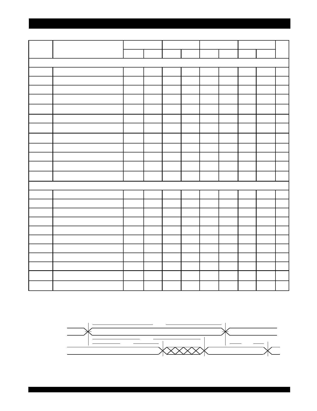
AC Electrical Characteristics (VDD = Min. to Max., Commercial and Industrial Temperature Ranges)
71T016SA10(2)
71T016SA12
71T016SA15
71T016SA20
Symbol
Parameter
Min.
Max.
Min.
Max.
Min.
Max.
Min.
Max. Unit
READ CYCLE
tRC
Read Cycle Time
10
____
12
____
15
____
20
____
ns
tAA
Address Access Time
____
10
____
12
____
15
____
20
ns
tACS
Chip Select Access Time
____
10
____
12
____
15
____
20
ns
tCLZ(1)
Chip Select Low to Output in Low-Z
4
____
4
____
5
____
5
____
ns
tCHZ(1)
Chip Select Hig h to Output in High-Z
____
5
____
6
____
6
____
8
ns
tOE
Output Enable Low to Output Valid
____
5
____
6
____
7
____
8
ns
tOLZ(1)
Output Enable Lo w to Output in Low-Z
0
____
0
____
0
____
0
____
ns
tOHZ(1)
Output Enable High to Output in High-Z
____
5
____
6
____
6
____
8
ns
tOH
Output Hold from Address Change
4
—
4
—
4
—
4
—
ns
tBE
Byte Enable Low to Output Valid
—
5
—
6
—
7
____
8
ns
tBLZ(1)
Byte Enable Low to Output in Low-Z
0
____
0
____
0
____
0
____
ns
tBHZ(1)
Byte Enable Hig h to Output in High-Z
____
5
____
6
____
6
____
8
ns
WRITE CYCLE
tWC
Write Cycle Time
10
____
12
____
15
____
20
____
ns
tAW
Address Valid to End of Write
7
____
8
____
10
____
12
____
ns
tCW
Chip Select Low to End of Write
7
____
8
____
10
____
12
____
ns
tBW
Byte Enable Low to End of Write
7
____
8
____
10
____
12
____
ns
tAS
Address Set-up Time
0
____
0
____
0
____
0
____
ns
tWR
Address Hold from End of Write
0
____
0
____
0
____
0
____
ns
tWP
Write Pulse Width
7
____
8
____
10
____
12
____
ns
tDW
Data Valid to End of Write
5
____
6
____
7
____
9
____
ns
tDH
Data Hold Time
0
____
0
____
0
____
0
____
ns
tOW(1)
Write Enable Hig h to Output in Low-Z
3
____
3
____
3
____
3
____
ns
tWHZ(1)
Write Enable Lo w to Output in High-Z
____
5
____
6
____
6
____
8
ns
NOTES:
1. This parameter is guaranteed with the AC Load (Figure 2) by device characterization, but is not production tested.
2. 00C to +700C temperature range only.
5326 tbl 10
Timing Waveform of Read Cycle No. 1(1,2,3)
ADDRESS
DATAOUT
tRC
tAA
tOH
PREVIOUS DATAOUT VALID
tOH
DATAOUT VALID
NOTES:
1. WE is HIGH for Read Cycle.
2. Device is continuously selected, CS is LOW.
3. OE, BHE, and BLE are LOW.
6.452
5326 drw 06
Share Link: 