SF104CTS 데이터 시트보기 (PDF) - Thinki Semiconductor Co., Ltd.
부품명
상세내역
제조사
SF104CTS
Thinki Semiconductor Co., Ltd.

SF104CTS Datasheet PDF : 2 Pages
| |||
SF101CTS thru SF108CTS
SF101CTS thru SF108CTS
Pb
Pb Free Plating Product
10.0 Ampere Heatsink Dual Series Connection Super Fast Recovery Rectifiers
Features
※ Fast switching for high efficiency
※ Low forward voltage drop
※ High current capability
※ Low reverse leakage current
※ High surge current capability
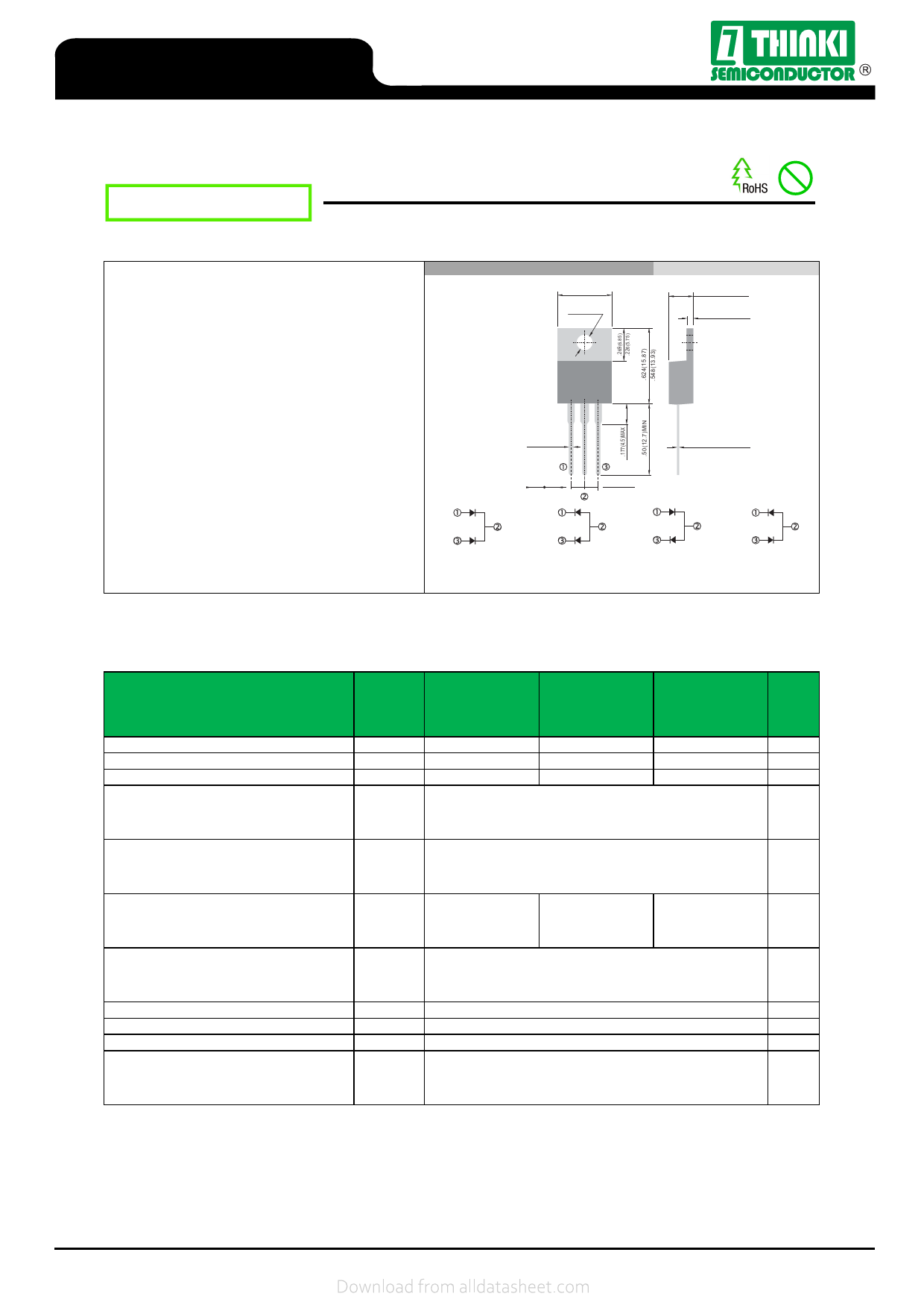
TO-220AB(TO-220-3L)
.419(10.66)
.387(9.85)
.139(3.55)
MIN
Unit:inch(mm)
.196(5.00)
.163(4.16)
.054(1.39)
.045(1.15)
Application
※ Automotive Inverters and Solar Inverters
※ Car Audio Amplifiers and Sound Device Systems
※ Plating Power Supply,Motor Control,UPS and SMPS etc.
Mechanical Data
※ Case: TO-220AB Open Metal Heatsink Package
※ Epoxy: UL 94V-0 rate flame retardant
※ Terminals: Solderable per MIL-STD-202 method 208
※ Polarity: As marked on diode body
※ Mounting position: Any
※ Weight: 2.2 gram approximately
.038(0.96)
.019(0.50)
.1(2.54)
.1(2.54)
.025(0.65)MAX
Case
Positive
Common Cathode
Suffix "CTG"
Case
Negative
Common Anode
Suffix "CTA"
Case
Doubler
Tandem Polarity
Suffix "CTD"
Case
Series
Tandem Polarity
Suffix "CTS"
MAXIMUM RATINGS AND ELECTRICAL CHARACTERISTICS
Rating at 25℃ ambient temperature unless otherwise specified.
Single phase,half wave,60Hz,resistive or inductive load.
For capacitive load, derate current by 20%.
PARAMETER
Maximum Recurrent Peak Reverse Voltage
Maximum RMS Voltage
Maximum DC Blocking Voltage
Maximum Average Forward Rectified
Current Tc=100 ℃
(Total Device 2x5.0A=10.0A)
Peak Forward Surge Current, 8.3ms single Half
sine-wave superimposed on rated load (JEDEC
method)
Maximum Instantaneous Forward Voltage
@5.0A
(Per Diode/Per Leg)
SYMBOL
VRRM
VRMS
VDC
IF(AV)
IFSM
VF
SF101CTS
SF104CTS
200
140
200
SF105CTS
SF106CTS
400
280
400
SF107CTS
SF108CTS
600
420
600
10.0
125
0.98
1.3
1.7
UNIT
V
V
V
A
A
V
Maximum DC Reverse Current @TJ=25℃
At Rated DC Blocking Voltage @TJ=125℃
IR
Maximum Reverse Recovery Time (Note1)
Typical Junction Capacitance (Note 2)
Typical Thermal Resistance (Note 3)
Trr
CJ
RθJC
Operating Junction and Storage
Temperature Range
TJ,TSTG
Note:(1)Reverse recovery test conditions IF = 0.5A, IR = 1.0A, Irr = 0.25A.
Note:(2)Measured at 1.0 MHz and applied reverse voltage of 4.0 Volts DC.
Note:(3)Thermal Resistance junction to case.
5.0
50
35
65
1.5
-55 to +150
μA
μA
nS
pF
℃/W
℃
Rev.10T
© 1995 Thinki Semiconductor Co., Ltd.
Page 1/2
http://www.thinkisemi.com.tw/
Share Link: