SL23HM3_A/H 데이터 시트보기 (PDF) - Vishay Semiconductors
부품명
상세내역
제조사
SL23HM3_A/H Datasheet PDF : 5 Pages
| |||
www.vishay.com
SL22, SL23
Vishay General Semiconductor
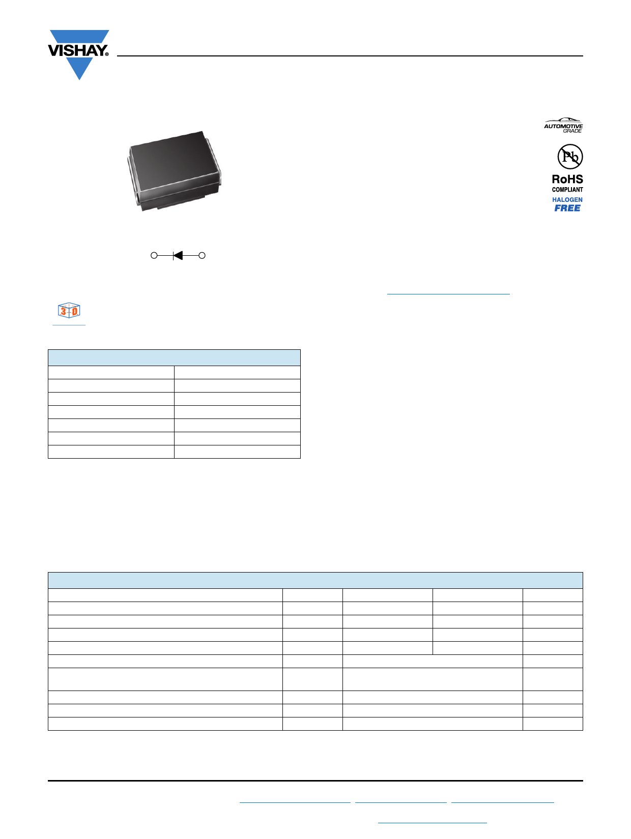
Surface-Mount Schottky Barrier Rectifier
SMB (DO-214AA)
Cathode
Anode
LINKS TO ADDITIONAL RESOURCES
3D 3D
3D Models
PRIMARY CHARACTERISTICS
IF(AV)
VRRM
IFSM
VF
TJ max.
Package
2.0 A
20 V, 30 V
100 A
0.32 V
125 °C
SMB (DO-214AA)
Circuit configuration
Single
FEATURES
• Low profile package
Available
• Ideal for automated placement
• Guardring for overvoltage protection
• Low power losses, high efficiency
• Very low forward voltage drop
• High surge capability
Available
• Meets MSL level 1, per J-STD-020, LF maximum peak
of 260 °C
• AEC-Q101 qualified available
- Automotive ordering code: base P/NHE3 or P/NHM3
• Material categorization: for definitions of compliance
please see www.vishay.com/doc?99912
TYPICAL APPLICATIONS
For use in low voltage high frequency inverters,
freewheeling, DC/DC converters, and polarity protection
applications.
MECHANICAL DATA
Case: SMB (DO-214AA)
Molding compound meets UL 94 V-0 flammability rating
Base P/N-E3 - RoHS-compliant, commercial grade
Base P/N-M3 - halogen-free, RoHS-compliant, commercial
grade
Base P/NHE3_X - RoHS-compliant and AEC-Q101 qualified
Base P/NHM3_X - halogen-free, RoHS-compliant, and
AEC-Q101 qualified
(“_X” denotes revision code e.g. A, B, .....)
Terminals: matte tin plated leads, solderable per
J-STD-002 and JESD 22-B102
E3, M3, HE3, and HM3 suffix meets JESD 201 class 2
whisker test
Polarity: color band denotes the cathode end
MAXIMUM RATINGS (TA = 25 °C unless otherwise noted)
PARAMETER
SYMBOL
Device marking code
Maximum repetitive peak reverse voltage
Maximum RMS voltage
VRRM
VRMS
Maximum DC blocking voltage
Maximum average forward rectified current at TL (fig.1)
Peak forward surge current 8.3 ms single half sine-wave
superimposed on rated load
VDC
IF(AV)
IFSM
Voltage rate of change (rated VR)
Operating junction temperature range
Storage temperature range
dV/dt
TJ
TSTG
SL22
SL23
SL2
SL3
20
30
14
21
20
30
2.0
100
10 000
-55 to +125
-55 to +150
UNIT
V
V
V
A
A
V/μs
°C
°C
Revision: 23-Apr-2020
1
Document Number: 88741
For technical questions within your region: DiodesAmericas@vishay.com, DiodesAsia@vishay.com, DiodesEurope@vishay.com
THIS DOCUMENT IS SUBJECT TO CHANGE WITHOUT NOTICE. THE PRODUCTS DESCRIBED HEREIN AND THIS DOCUMENT
ARE SUBJECT TO SPECIFIC DISCLAIMERS, SET FORTH AT www.vishay.com/doc?91000
Share Link: 