M5M5256DFP-70G 데이터 시트보기 (PDF) - Renesas Electronics
부품명
상세내역
제조사
M5M5256DFP-70G Datasheet PDF : 8 Pages
| |||
RENESAS LSIs
M5M5256DFP,VP -70G,-70GI,-70XG
262144-BIT (32768-WORD BY 8-BIT) CMOS STATIC RAM
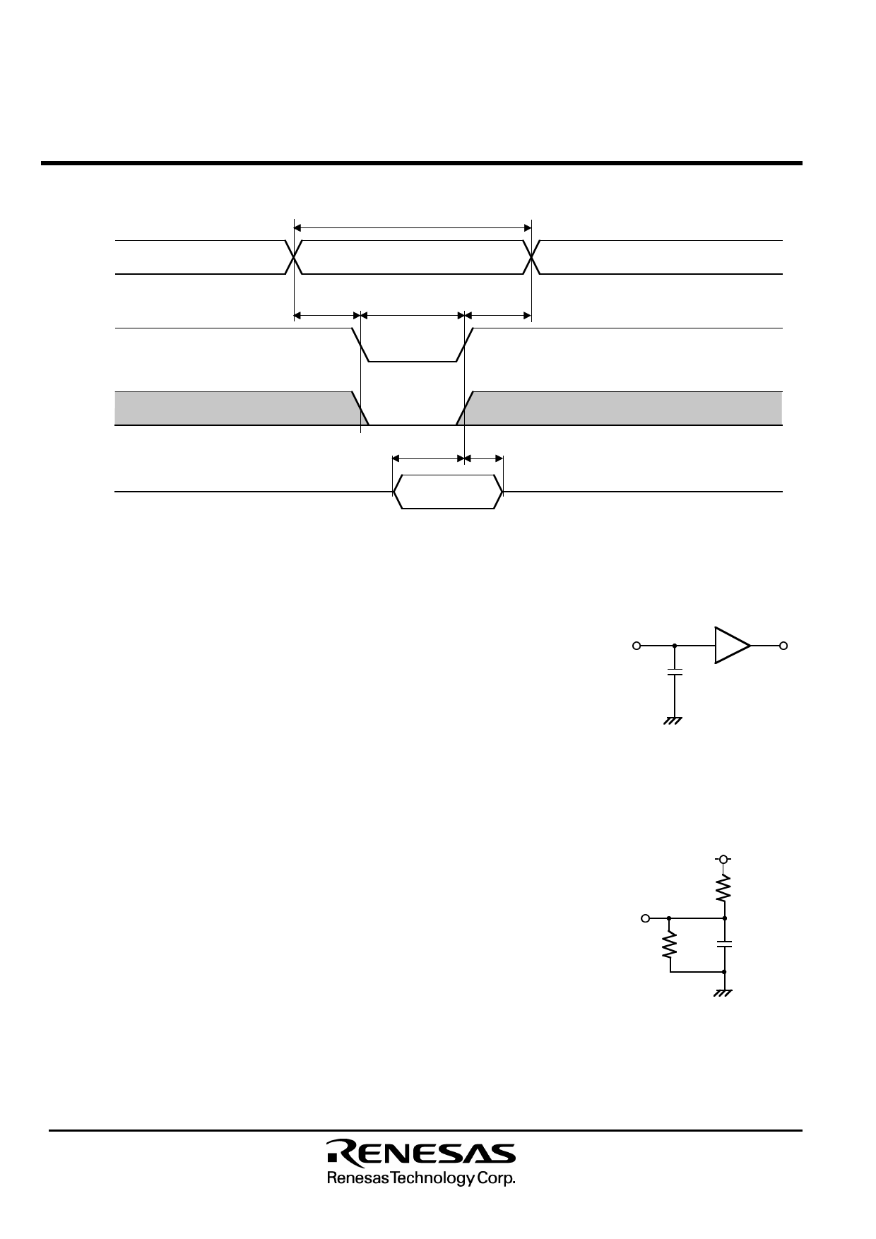
Write cycle ( /S control mode)
tCW
A 0~ 14
tsu (A)
tsu (S)
trec (W)
/S
/W
DQ1~ 8
(Note 5)
(Note 3)
(Note 4)
tsu (D) th (D)
DATA IN
STABLE
(Note 3)
(4) MEASUREMENT CONDITIONS
Limits1:Vcc=3.3±0.3V
Input pulse level .............. VIH=2.4V,VIL=0.4V
Input rise and fall time ..... 5ns
Reference level ................ VOH=VOL=1.5V
Output load ...................... Fig.1, CL=30pF
CL=5pF (for ten,tdis)
T ransition is measured ±500mV from steady
state voltage. (for ten,tdis)
DQ
CL
(Including
scope and JIG)
Fig.1 Output load
Limits2:Vcc=5.0±0.5V
Input pulse level .............. VIH=2.4V,VIL=0.6V
Input rise and fall time ..... 5ns
Reference level ................ VOH=VOL=1.5V
Output load ...................... Fig.2, CL=100pF
CL=5pF (for ten,tdis)
T ransition is measured ±500mV from steady
state voltage. (for ten,tdis)
DQ
(Including
scope and JIG)
Vcc
1.8k Ω
990Ω CL
Fig.2 Output load
Note 3 : Hatching indicates the state is "don't care".
4 : Writing is executed in ov erlap of /S and /W low.
5 : If /W goes low simultaneously with or prior to /S, the outputs remain in the high impedance state.
6 : Don't apply inv erted phase signal externally when DQ pin is output mode.
7 : ten, tdis are periodically sampled and are not 100% tested.
6
Share Link: 