PI74FCT16260TA 데이터 시트보기 (PDF) - Pericom Semiconductor
부품명
상세내역
제조사
PI74FCT16260TA Datasheet PDF : 5 Pages
| |||
PI74FCT16260T
PI74FCT162260T 1122334455667788990011223344556677889900112233445566778899001122112233445566778899001122334455667788990011223344556677889900112211223344556677889900112233445566778899001122334455667788990011221122334455667788990011223344556677889900112233445566778899001122112233445566778899001122
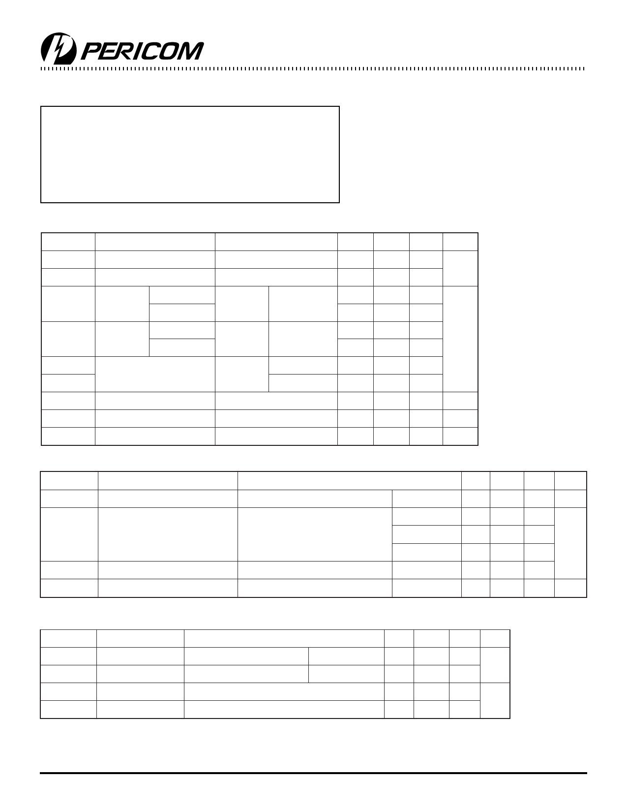
Maximum Ratings
Fast CMOS 12-Bit Tri-Port Bus Exchanger
(Above which the useful life may be impaired. For user guidelines, not tested.)
Storage Temperature ........................................................ 65°C to +150°C
Ambient Temperature with Power Applied ...................... 40°C to +85°C
Input Voltage Range, VIN ......................................... 0.5V to VCC +0.5V
Output Voltage Range, VOUT ................................... 0.5V to VCC +0.5V
DC Input Voltage ............................................................... 0.5V to +5.0V
DC Output Current .......................................................................... 100 mA
Power Dissipation ............................................................................... 1.0W
Note:
Stresses greater than those listed under MAXIMUM
RATINGS may cause permanent damage to the device.
This is a stress rating only and functional operation of the
device at these or any other conditions above those indi-
cated in the operational sections of this specification is not
implied. Exposure to absolute maximum rating conditions
for extended periods may affect reliability.
DC Electrical Characteristics (Over the Operating Range, TA = 40°C to +85°C, VCC =5.0V ± 10%)
Parameters
Description
Test Conditions(1) Min. Typ.(2) Max. Units
VIH
Input High Voltage
Guaranteed Logic HIGH Level 2.0
VIL
Input LOW Voltage
Guaranteed Logic LOW Level
IIH
Input HIGH
Current
(Input pins)
(I/O pins)
VCC = Max.
VIN = VCC
V
0.8
-1
-1
IIL
Input LOW
Current
(Input pins)
(I/O pins)
VCC = Max.
VIN = Max.
-1
mA
-1
IOZH
IOZL
High Impedeance
Output Current
VOUT = 2.7V
VCC = Max.
VOUT = 0.5V
-1
-1
VIK
Clamp Diode Voltage
VCC = Min., IIN = -18mA
-0.7 -1.2 V
IOS
Short Circuit Current (I/O pins) VCC = Max.(3), VOUT = GND -80
-140 -250 mA
VH
Input Hysteresis
100
mV
PI74FCT16260T Output Drive Characteristics (Over the Operating Range)
Parameters
Description
IO
Output Drive Current (I/O pins)
Test Conditions(1)
VCC = Max.(3), VOUT = 2.5V
Min. Typ.(2) Max. Units
-50
-180 mA
VOH
Output High Voltage
VCC = Min.,
VIN = VIH = VIH or VIL
IOH = -3.0mA 2.5 3.5
IOH = -15.0mA 2.4 3.5
V
IOH = -32.0mA 2.0 3.0
VOL
Output LOW Voltage
VCC = Min., VIN = VIH = VIH or VIL IOL = 64mA
0.2 0.55
IOFF
Input /Output Power OFF Leakage VCCC = 0V, VIN or VOUT ≤ 4.5V
±1 mA
PI74FCT162260T Output Drive Characteristics (Over the Operating Range)
Parameters
Description
Test Conditions(1)
Min. Typ.(2) Max. Units
VOH
VOL
Output High Voltage VCC = Min., VIN = VIH or VIL IOH = -24.0mA 2.4
Output LOW Voltage VCC = Min., VIN = VIH or VIL IOL = 24.0mA
3.3
V
0.3 0.55
IODL
IODH
Output LOW Current
Output HIGH Current
VCC = 5V, VIN = VIH or VIL, VOUT = 1.5V(3)
VCC = 5V, VIN = VIH or VIL, VOUT = 1.5V(3)
60 115 200
mA
-60 -115 -200
Notes:
1. For Max. or Min. conditions, use appropriate value specified under Electrical Characteristics for the applicable device type.
2. Typical values are at Vcc = 5.0V, +25ºC ambient and maximum loading.
3. Not more than one output should be shorted at one time. Duration of the test should not exceed one second.
3
PS8307A 11/17/98
Share Link: 