SM12T1(2017) 데이터 시트보기 (PDF) - ON Semiconductor
부품명
상세내역
제조사
SM12T1 Datasheet PDF : 7 Pages
| |||
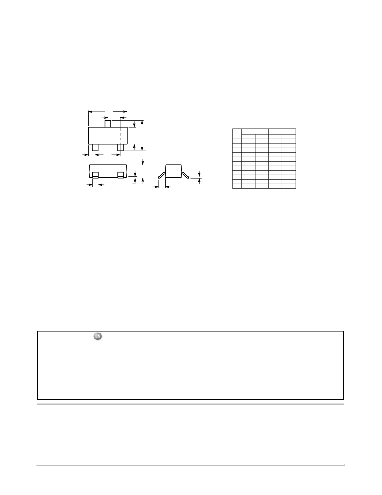
MECHANICAL CASE OUTLINE
PACKAGE DIMENSIONS
SCALE 4:1
D
3
E
1
2
e
TOP VIEW
A
A1
SIDE VIEW
SOT−23 (TO−236)
CASE 318−08
ISSUE AS
DATE 30 JAN 2018
HE
3X b
0.25
T
L
L1
VIEW C
SEE VIEW C
c
END VIEW
NOTES:
1. DIMENSIONING AND TOLERANCING PER ASME Y14.5M, 1994.
2. CONTROLLING DIMENSION: MILLIMETERS.
3. MAXIMUM LEAD THICKNESS INCLUDES LEAD FINISH.
MINIMUM LEAD THICKNESS IS THE MINIMUM THICKNESS OF
THE BASE MATERIAL.
4. DIMENSIONS D AND E DO NOT INCLUDE MOLD FLASH,
PROTRUSIONS, OR GATE BURRS.
MILLIMETERS
DIM MIN NOM MAX
A 0.89
1.00
1.11
A1 0.01
0.06
0.10
b
0.37
0.44
0.50
c
0.08
0.14
0.20
D 2.80
2.90
3.04
E 1.20
1.30
1.40
e
1.78
1.90
2.04
L 0.30
0.43
0.55
L1 0.35
0.54
0.69
H E 2.10
T
0°
2.40
−−−
2.64
10°
MIN
0.035
0.000
0.015
0.003
0.110
0.047
0.070
0.012
0.014
0.083
0°
INCHES
NOM
0.039
0.002
0.017
0.006
0.114
0.051
0.075
0.017
0.021
0.094
−−−
MAX
0.044
0.004
0.020
0.008
0.120
0.055
0.080
0.022
0.027
0.104
10°
GENERIC
MARKING DIAGRAM*
RECOMMENDED
SOLDERING FOOTPRINT
XXXMG
G
1
2.90
3X
0.90
XXX = Specific Device Code
M = Date Code
G = Pb−Free Package
3X 0.80
0.95
PITCH
DIMENSIONS: MILLIMETERS
*This information is generic. Please refer to
device data sheet for actual part marking.
Pb−Free indicator, “G” or microdot “ G”,
may or may not be present.
STYLE 1 THRU 5:
CANCELLED
STYLE 9:
PIN 1. ANODE
2. ANODE
3. CATHODE
STYLE 6:
PIN 1. BASE
2. EMITTER
3. COLLECTOR
STYLE 10:
PIN 1. DRAIN
2. SOURCE
3. GATE
STYLE 7:
PIN 1. EMITTER
2. BASE
3. COLLECTOR
STYLE 8:
PIN 1. ANODE
2. NO CONNECTION
3. CATHODE
STYLE 11:
STYLE 12:
PIN 1. ANODE
PIN 1. CATHODE
2. CATHODE
2. CATHODE
3. CATHODE−ANODE
3. ANODE
STYLE 13:
PIN 1. SOURCE
2. DRAIN
3. GATE
STYLE 14:
PIN 1. CATHODE
2. GATE
3. ANODE
STYLE 15:
PIN 1. GATE
2. CATHODE
3. ANODE
STYLE 16:
PIN 1. ANODE
2. CATHODE
3. CATHODE
STYLE 17:
PIN 1. NO CONNECTION
2. ANODE
3. CATHODE
STYLE 18:
STYLE 19:
STYLE 20:
PIN 1. NO CONNECTION PIN 1. CATHODE
PIN 1. CATHODE
2. CATHODE
2. ANODE
2. ANODE
3. ANODE
3. CATHODE−ANODE
3. GATE
STYLE 21:
PIN 1. GATE
2. SOURCE
3. DRAIN
STYLE 27:
PIN 1. CATHODE
2. CATHODE
3. CATHODE
STYLE 22:
PIN 1. RETURN
2. OUTPUT
3. INPUT
STYLE 28:
PIN 1. ANODE
2. ANODE
3. ANODE
STYLE 23:
PIN 1. ANODE
2. ANODE
3. CATHODE
STYLE 24:
PIN 1. GATE
2. DRAIN
3. SOURCE
STYLE 25:
PIN 1. ANODE
2. CATHODE
3. GATE
STYLE 26:
PIN 1. CATHODE
2. ANODE
3. NO CONNECTION
DOCUMENT NUMBER: 98ASB42226B
DESCRIPTION: SOT−23 (TO−236)
Electronic versions are uncontrolled except when accessed directly from the Document Repository.
Printed versions are uncontrolled except when stamped “CONTROLLED COPY” in red.
PAGE 1 OF 1
ON Semiconductor and
are trademarks of Semiconductor Components Industries, LLC dba ON Semiconductor or its subsidiaries in the United States and/or other countries.
ON Semiconductor reserves the right to make changes without further notice to any products herein. ON Semiconductor makes no warranty, representation or guarantee regarding
the suitability of its products for any particular purpose, nor does ON Semiconductor assume any liability arising out of the application or use of any product or circuit, and specifically
disclaims any and all liability, including without limitation special, consequential or incidental damages. ON Semiconductor does not convey any license under its patent rights nor the
rights of others.
© Semiconductor Components Industries, LLC, 2019
www.onsemi.com
Share Link: 