ADSP-BF518F16 데이터 시트보기 (PDF) - Analog Devices
부품명
상세내역
제조사
ADSP-BF518F16 Datasheet PDF : 68 Pages
| |||
Blackfin
Embedded Processor
ADSP-BF512/BF514/BF514F16/BF516/BF518/BF518F16
FEATURES
Up to 400 MHz high performance Blackfin processor
Two 16-bit MACs, two 40-bit ALUs, four 8-bit video ALUs,
40-bit shifter
RISC-like register and instruction model for ease of
programming and compiler-friendly support
Advanced debug, trace, and performance monitoring
Wide range of operating voltages. See Operating Conditions
on Page 22
Qualified for Automotive Applications. See Automotive
Products on Page 67
168-ball CSP_BGA or 176-lead LQFP_EP (with exposed pad)
MEMORY
116K bytes of on-chip memory
External memory controller with glueless support for SDRAM
and asynchronous 8-bit and 16-bit memories
Optional 16M bit SPI flash with boot option
Flexible booting options from internal SPI flash, OTP
memory, external SPI/parallel memories, or from SPI/UART
host devices
Code security with Lockbox secure technology
One-time-programmable (OTP) memory
Memory management unit providing memory protection
PERIPHERALS
IEEE 802.3-compliant 10/100 Ethernet MAC with IEEE 1588
support (ADSP-BF518/ADSP-BF518F16 only)
Parallel peripheral interface (PPI), supporting ITU-R 656
video data formats
2 dual-channel, full-duplex synchronous serial ports
(SPORTs), supporting 8 stereo I2S channels
12 peripheral DMAs, 2 mastered by the Ethernet MAC
2 memory-to-memory DMAs with external request lines
Event handler with 56 interrupt inputs
2 serial peripheral interfaces (SPI)
Removable storage interface (RSI) controller for MMC, SD,
SDIO, and CE-ATA
2 UARTs with IrDA support
2-wire interface (TWI) controller
Eight 32-bit timers/counters with PWM support
3-phase 16-bit center-based PWM unit
32-bit general-purpose counter
Real-time clock (RTC) and watchdog timer
32-bit core timer
40 general-purpose I/Os (GPIOs)
Debug/JTAG interface
On-chip PLL capable of frequency multiplication
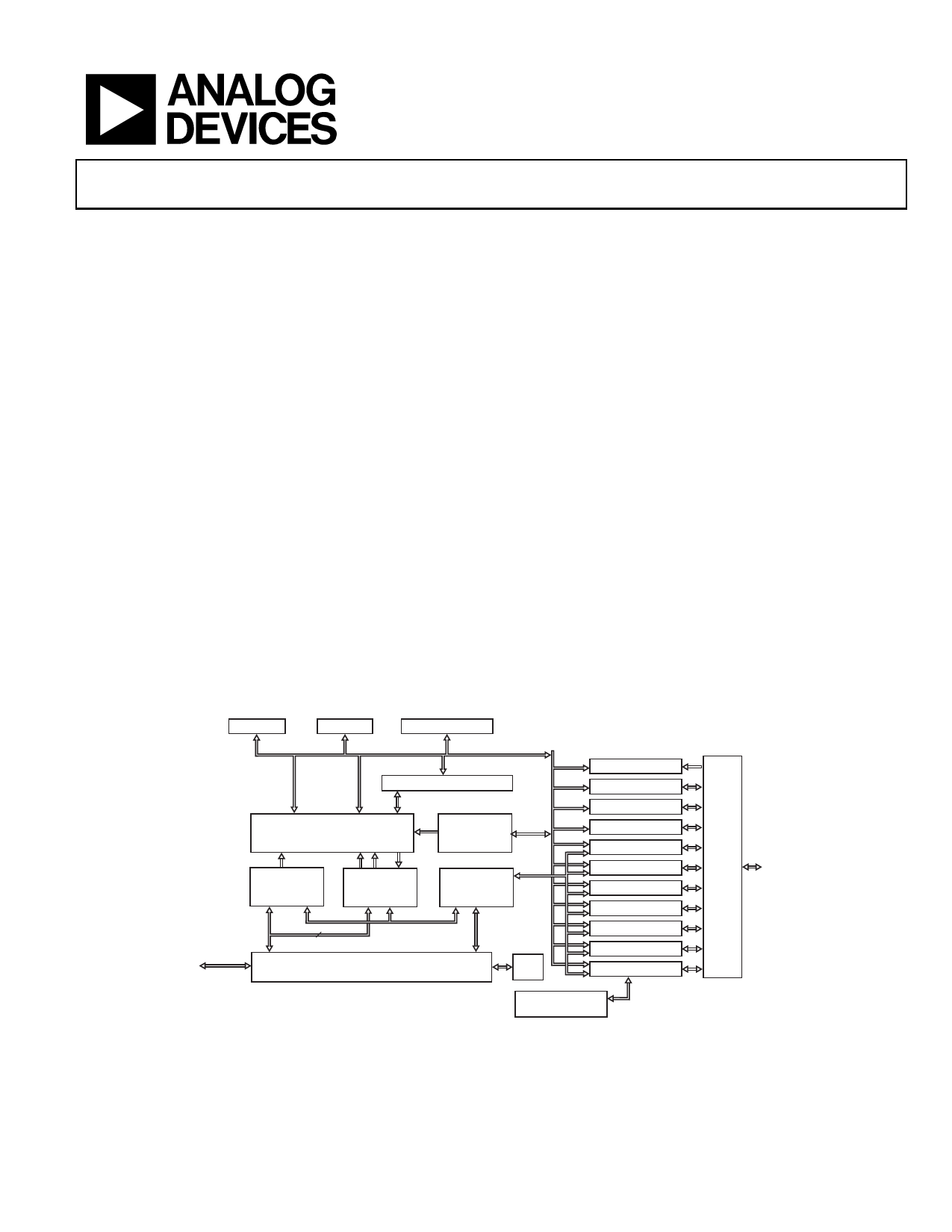
RTC
OTP
WATCHDOG TIMER
PERIPHERAL
ACCESS BUS
JTAG TEST AND EMULATION
B
INTERRUPT
CONTROLLER
L1
INSTRUCTION
MEMORY
L1
DATA
MEMORY
DMA
CONTROLLER
16
DMA CORE BUS
EXTERNAL ACCESS BUS
DMA
EXTERNAL
BUS
EXTERNAL PORT
FLASH, SDRAM CONTROL
BOOT
ROM
COUNTER
3-PHASE PWM
TIMER7–0
TWI
SPORT1-0
RSI (SDIO)
PPI
UART1–0
EMAC
SPI1
SPI0
16M bit SPI Flash
(See Table 1)
Figure 1. Functional Block Diagram
PORTS
Blackfin and the Blackfin logo are registered trademarks of Analog Devices, Inc.
Rev. D
Document Feedback
Information furnished by Analog Devices is believed to be accurate and reliable.
However, no responsibility is assumed by Analog Devices for its use, nor for any
infringements of patents or other rights of third parties that may result from its use.
Specifications subject to change without notice. No license is granted by implication
or otherwise under any patent or patent rights of Analog Devices. Trademarks and
registered trademarks are the property of their respective owners.
One Technology Way, P.O. Box 9106, Norwood, MA 02062-9106 U.S.A.
Tel: 781.329.4700
©2014 Analog Devices, Inc. All rights reserved.
Technical Support
www.analog.com
Share Link: 