SIHFI9530G 데이터 시트보기 (PDF) - VBsemi Electronics Co.,Ltd
부품명
상세내역
제조사
SIHFI9530G Datasheet PDF : 7 Pages
| |||
SiHFI9530G
P-Channel 100 V (D-S) MOSFET
www.VBsemi.tw
PRODUCT SUMMARY
VDS (V)
RDS(on) (Ω)
- 100
0.220 at VGS = - 10 V
0.230 at VGS = - 4.5 V
ID (A)
- 12
- 10
Qg (Typ.)
11.7
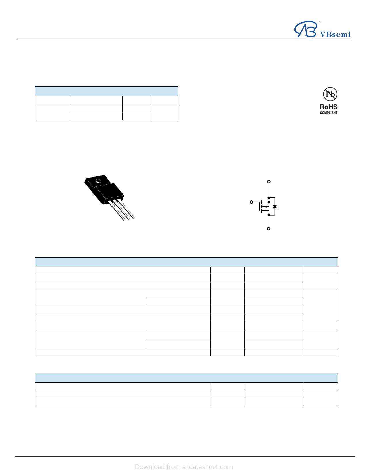
TO-220 FULLPAK
FEATURES
• Halogen-free According to IEC 61249-2-21
Definition
• TrenchFET® Power MOSFET
• 100 % Rg and UIS Tested
• Compliant to RoHS Directive 2002/95/EC
APPLICATIONS
• Power Switch
• DC/DC Converters
S
G
GDS
Top View
D
P-Channel MOSFET
ABSOLUTE MAXIMUM RATINGS TC = 25 °C, unless otherwise noted
Parameter
Symbol
Drain-Source Voltage
VDS
Gate-Source Voltage
VGS
Continuous Drain Current (TJ = 150 °C)
TC = 25 °C
TC = 70 °C
ID
Pulsed Drain Current
IDM
Avalanche Current
IAS
Single Avalanche Energya
L = 0.1 mH
EAS
Maximum Power Dissipationa
TC = 25 °C
TA = 25 °Cc
PD
Operating Junction and Storage Temperature Range
TJ, Tstg
Limit
- 100
± 20
- 12
- 8.6
- 36
- 18
16.2
38.1b
2.5
- 55 to 150
THERMAL RESISTANCE RATINGS
Parameter
Junction-to-Ambient (PCB Mount)c
Junction-to-Case (Drain)
Notes:
a. Duty cycle ≤ 1 %.
b. See SOA curve for voltage derating.
c. When Mounted on 1" square PCB (FR-4 material).
Symbol
RthJA
RthJC
Limit
50
3.9
Unit
V
A
mJ
W
°C
Unit
°C/W
E-mail:China@VBsemi TEL:86-755-83251052
1
Share Link: 