BR24A04-WM(2009) 데이터 시트보기 (PDF) - ROHM Semiconductor
부품명
상세내역
제조사
BR24A04-WM Datasheet PDF : 18 Pages
| |||
BR24A□□-WM series
Technical Note
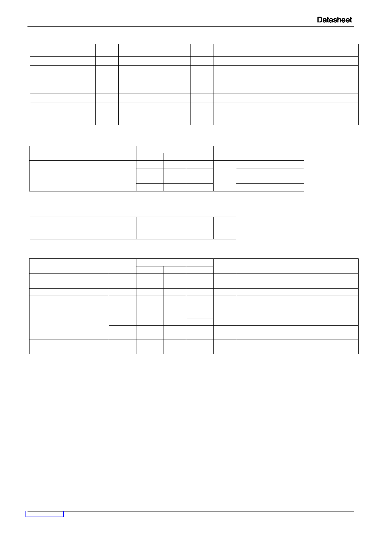
●Absolute maximum ratings (Ta=25℃)
Parameter
symbol
Limits
Unit
Impressed voltage
Permissible dissipation
VCC
Pd
-0.3~+6.5
V
450 (SOP8) *1
450 (SOP-J8) *2
mW
310 (MSOP8) *3
Storage temperature range
Tstg
-65~+125
℃
Action temperature range
Topr
-40~+105
℃
Terminal voltage
-
-0.3~VCC+1.0
V
When using at Ta=25℃ or higher, 4.5mW(*1,*2) , 3.1mW(*3) to be reduced per 1℃
●Memory cell characteristics (VCC=2.5~5.5V)
Parameter
Number of data rewrite times *1
Data hold years *1
○Shipment data all address FFh
*1 Not 100% TESTED
Min.
100,000
40
Limits
Typ.
-
-
Max.
-
-
Unit
Times
Years
Test Condition
Ta=-40~105℃
Ta=25℃
●Recommended operating conditions
Parameter
Symbol
Limits
Unit
Power source voltage
Input voltage
VCC
VIN
2.5~5.5
0~VCC
V
●Electrical characteristics (Unless otherwise specified, Ta=-40~+105℃, VCC=2.5~5.5V)
Parameter
Symbol
Limits
Min. Typ. Max.
Unit
Conditions
“HIGH” input voltage
VIH
0.7VCC -
-
V
“LOW” input voltage
VIL
-
- 0.3 VCC
V
“LOW” output voltage 1 VOL
-
-
0.4
V IOL=3.0mA (SDA)
Input leak current
ILI
-1
-
1
μA VIN=0V~VCC
Output leak current
ILO
-1
-
1
μA VOUT=0V~VCC, (SDA)
Current consumption
ICC1
-
-
2.0 *1
3.0 *2
mA
VCC=5.5V,fSCL=400kHz, tWR=5ms,
Byte write, Page write
at action
ICC2
-
-
0.5
mA
VCC=5.5V,fSCL=400kHz
Random read, current read, sequential read
Standby current
ISB
-
-
2.0
μA
VCC=5.5V, SDA・SCL=VCC
A0, A1, A2=GND, WP=GND
◎Radiation resistance design is not made.
*1 BR24A01A/02/04/08/16-WM, *2 BR24A32/64-WM
●Action timing characteristics (Unless otherwise specified, Ta=-40~+105℃, VCC=2.5~5.5V)
FAST-MODE
STANDARD-MODE
Parameter
Symbol
2.5V≦VCC≦5.5V
2.5V≦VCC≦5.5V
Unit
Min. Typ. Max. Min. Typ. Max.
SCL frequency
fSCL
-
-
400
-
-
100 kHz
Data clock “HIGH“ time
tHIGH
0.6
-
-
4.0
-
-
μs
Data clock “LOW“ time
SDA, SCL rise time *1
SDA, SCL fall time *1
tLOW
1.2
-
-
4.7
-
-
μs
tR
-
-
0.3
-
-
1.0
μs
tF
-
-
0.3
-
-
0.3
μs
Start condition hold time
tHD:STA
0.6
-
-
4.0
-
-
μs
Start condition setup time
tSU:STA
0.6
-
-
4.7
-
-
μs
Input data hold time
tHD:DAT
0
-
-
0
-
-
ns
Input data setup time
tSU:DAT 100
-
-
250
-
-
ns
Output data delay time
tPD
0.1
-
0.9
0.2
-
3.5
μs
Output data hold time
tDH
0.1
-
-
0.2
-
-
μs
Stop condition setup time
tSU:STO
0.6
-
-
4.7
-
-
μs
Bus release time before transfer start
tBUF
1.2
-
-
4.7
-
-
μs
Internal write cycle time
tWR
-
-
5
-
-
5
ms
Noise removal valid period (SDA, SCL terminal)
tI
-
-
0.1
-
-
0.1
μs
WP hold time
tHD:WP
0
-
-
0
-
-
ns
WP setup time
tSU:WP
0.1
-
-
0.1
-
-
μs
WP valid time
tHIGH:WP 1.0
-
-
1.0
-
-
μs
*1 Not 100% tested
www.rohm.com
© 2009 ROHM Co., Ltd. All rights reserved.
2/17
2009.08 - Rev.C
Share Link: 