BR24T02-WG 데이터 시트보기 (PDF) - ROHM Semiconductor
부품명
상세내역
제조사
BR24T02-WG Datasheet PDF : 38 Pages
| |||
BR24T02-W
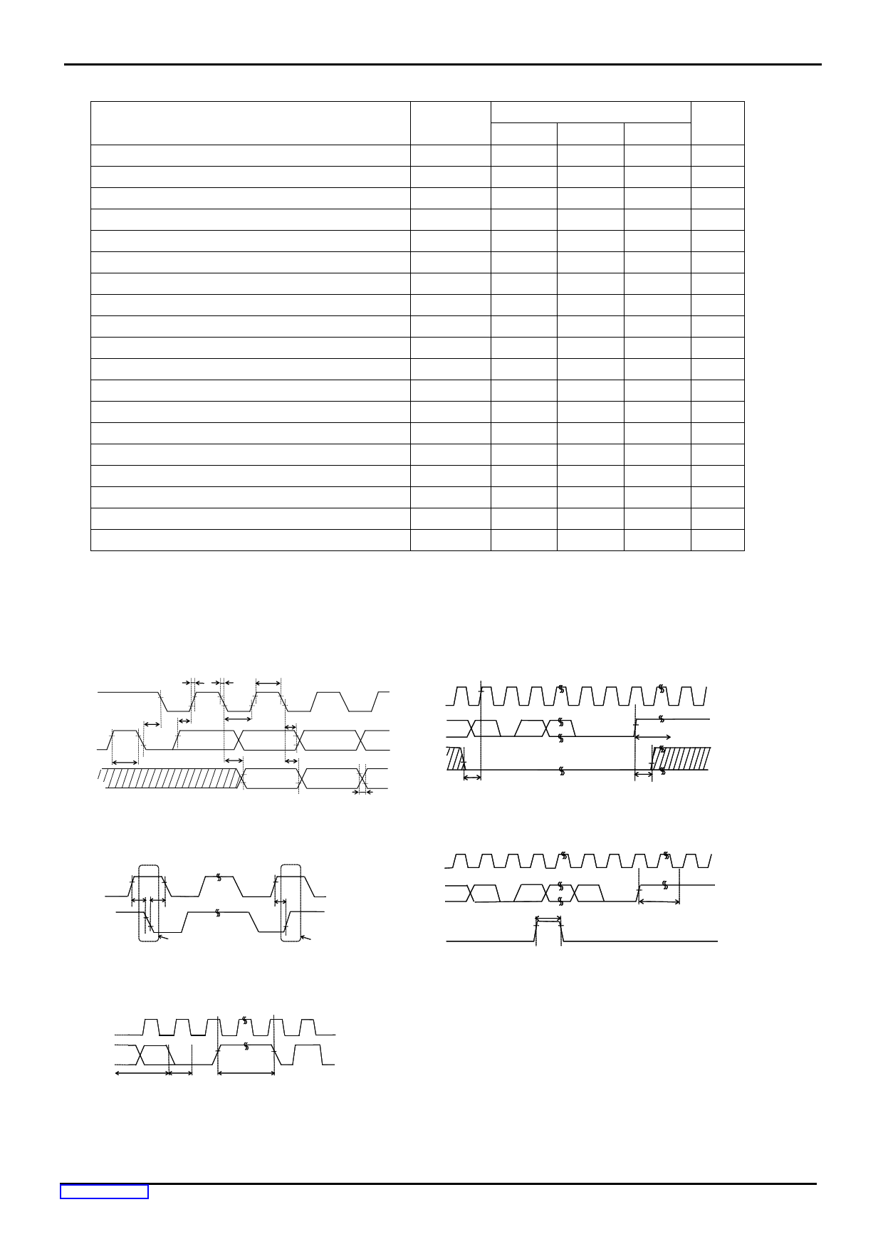
AC Characteristics (Unless otherwise specified, Ta= -40°C to +85°C, VCC=1.6V to 5.5V)
Parameter
Limit
Symbol
Min
Typ
Max
Clock Frequency
fSCL
-
-
400
Data Clock High Period
tHIGH
0.6
-
-
Data Clock Low Period
tLOW
1.2
-
-
SDA,SCL(INPUT) Rise Time (1)
tR
-
-
1.0
SDA,SCL (INPUT)Fall Time (1)
tF1
-
-
1.0
SDA(OUTPUT)Fall Time (1)
tF2
-
-
0.3
Start Condition Hold Time
tHD:STA
0.6
-
-
Start Condition Setup Time
tSU:STA
0.6
-
-
Input Data Hold Time
tHD:DAT
0
-
-
Input Data Setup Time
tSU:DAT
100
-
-
Output Data Delay Time
tPD
0.1
-
0.9
Output Data Hold Time
tDH
0.1
-
-
Stop Condition Setup Time
tSU:STO
0.6
-
-
Bus Free Time
tBUF
1.2
-
-
Write Cycle Time
tWR
-
-
5
Noise Spike Width (SDA and SCL)
tI
-
-
0.1
WP Hold Time
tHD:WP
1.0
-
-
WP Setup Time
tSU:WP
0.1
-
-
WP High Period
tHIGH:WP
1.0
-
-
(1) Not 100% TESTED.
Condition Input Data Level:VIL=0.2×VCC VIH=0.8×VCC
Input Data Timing Reference Level: 0.3×VCC/0.7×VCC
Output Data Timing Reference Level: 0.3×VCC/0.7×VCC
Rise/Fall Time : ≤20ns
Datasheet
Unit
kHz
µs
µs
µs
µs
µs
µs
µs
ns
ns
µs
µs
µs
µs
ms
µs
µs
µs
µs
Serial Input / Output Timing
tR
tF1
tHIGH
SCL
70%
SDA
((I入NP力U) T)
tHD:STA
70%
30%
tBUF
70%
70% 70%
30%
30%
tSU:DAT
tLOW
70%
tPD
70%
30%
70%
30%
tHD:DAT
70%
30%
tDH
SDA
70%
((O出U力T)PUT)
30%
30%
SDA ○Input read at the rise edge of S70C% L 70%
(output)○Data
output
in
sync
with
the
30%
fall of
SCL30%
70%
30%
tF2
Figure 2-(a). Serial Input / Output Timing
70%
DATA(1)
D1
D0 ACK
DATA(n)
ACK
70%
tWR
30%
30%
ttSSUU::WWPP
tHD:WPP
SSTTOOPP CCOONNDDIITTIIOONN
Figure 2-(d). WP Timing at Write Execution
70%
70%
70%
tSU:STA
tHD:STA
70%
30%
START CONDITION
tSU:STO
30%
STOP CONDITION
30%
30%
FigureST2AR-T(CbON)D.ITSIONtart-Stop Bit Timing STOP CONDITION
DDAATTAA((11))
DDAATTAA((nn))
DD11
DD00 AACCKK
ttHHIIGGHH::WWPP
Fig1-(4) Write7700c%%ycle tim77i00n%%g
AACCKK
7700%%
ttWWRR
Fig1-(5) WP timing at write execution
Fig1-F(6i)guWrPe t2im-(ieng).aWt wPritTeimcainncgel at Write Cancel
D0
write data
(n-th address)
ACK
70%
70%
tWR
STOP CONDITION START CONDITION
Figure 2-(c). Write Cycle Timing
www.rohm.com
©2013 ROHM Co., Ltd. All rights reserved.
TSZ22111 • 15 • 001
Fig1-(5) WP timing at write execution
Fig1-(6) WP timing at write cancel
3/33
TSZ02201-0R2R0G100070-1-2
25.Dec.2020 Rev.008
Share Link: 