MPC9120 데이터 시트보기 (PDF) - Motorola => Freescale
부품명
상세내역
제조사
MPC9120 Datasheet PDF : 6 Pages
| |||
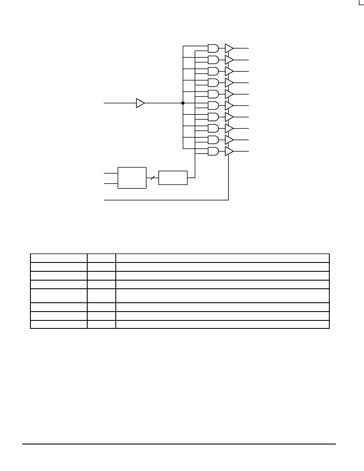
MPC9120
BUF_IN
SDATA
SCLOCK
OE
I2C
10
CONFIG
INTERFACE
REGISTERS
Figure 2. Block Diagram
SDRAM0
SDRAM1
SDRAM2
SDRAM3
SDRAM4
SDRAM5
SDRAM6
SDRAM7
SDRAM8
SDRAM9
Table 1. Pin Descriptions
Pin Name
I/O
BUF_IN
I
SDRAM0:9
O
SDATA
I/O
SCLK
I
OE
I
VDD
–
VSS
–
Function
3.3V CMOS clock input
3.3V CMOS SDRAM clock outputs
Serial data for configuration control
Serial clock input for configuration control. The state of the SDATA input is clocked into the device on
the rising edge of this clock
A Low forces all outputs into High–Z state
3.3V power supply connection
Ground connection which should be connected directly to the ground plane
MOTOROLA
2
TIMING SOLUTIONS
BR1333 — REV 5
Share Link: 