MOCZ500 데이터 시트보기 (PDF) - Motorola => Freescale
부품명
상세내역
제조사
MOCZ500 Datasheet PDF : 8 Pages
| |||
MOCZ500
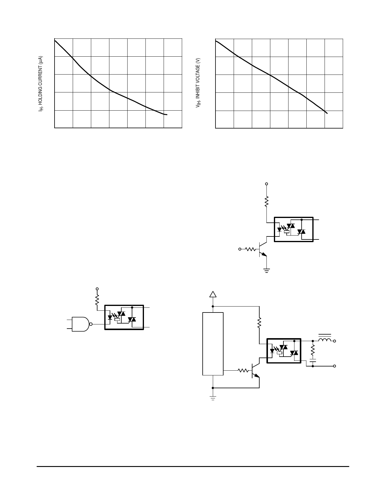
300
TYPICAL ELECTRICAL CHARACTERISTICS (continued)
11.5
250
11
200
10.5
150
10
100
9.5
50
– 40 – 20
0
20
40
60
80 100
TA, AMBIENT TEMPERATURE (°C)
Figure 7. Holding Current versus
Ambient Temperature
9
– 40 – 20
0
20
40
60
80 100
TA, AMBIENT TEMPERATURE (°C)
Figure 8. Inhibit Voltage versus
Ambient Temperature
APPLICATION CONSIDERATIONS
Input Drive Circuit
The MOCZ500 SSR is guaranteed to trigger with an input
VCC
current of 10 mA at 25°C. This trigger current increases with
lower ambient temperatures as shown on Figure 3 Forward
Trigger Current (IFT) versus Ambient Temperature.
When the input drive circuit is capable to supply the
R1
MOCZ500
MOCZ500 input LED trigger current, only a current limiting
resistor in series with the LED is required. TTL, DTL and
microcontrollers with enhanced current capability output
ports are able to meet this requirement.
Most CMOS logic circuits and Microcontroller output
ports are not rated to sink or source currents required to
R2
Vin
Q1
trigger the MOCZ500. In this case a drive circuit is required
as shown in Figure 10 or a TTL buffer interface circuit as
shown in Figure 9.
Figure 10. Noninverting Discrete NPN Buffer
VCC
and Level Shifter
R1
VCC
TTI/DTL
R1 for VCC (low) 4.5 V, IFT = 10 mA, VF LED = 1.2 V, VOL = 0.5 V
R1 = (4.5 V – 1.2 V – 0.5 V): 10 mA = 280 Ω
Choose 270 Ω
Figure 9. Input Drive Circuit
Snubber Circuit
Snubberless operation of resistive loads is possible, but
snubbers are recommended for all applications. A typical ap-
plication is shown in Figure 11. The snubber attenuates the
high kickback voltages and commutating dv/dt generated by
inductive loads during the turn off of the SSR. It also protects
the SSR from line transients generated elsewhere within the
equipment (for example inductive loads switched by me-
chanical contacts such as relays manual on/off switches etc.)
or outside the equipment such as air conditioners, electrical
heaters and motors.
R1
MOCZ500
LOAD
µP
R2
Q1
Rs AC LINE
Cs
Buffer Circuit
R1 = (VCC – VFLED – Vsat Q1): IF MOCZ500
R2 = 10 kΩ
Q1 = General Purpose Trans. NPN
Typical Snubber circuit:
For inductive and resistive loads Rs = 45 Ω Cs = 0.01 µF
Figure 11. Typical Application with an µP Output Buffer
4
Motorola Optoelectronics Device Data
Share Link: 