STP6NB80 데이터 시트보기 (PDF) - STMicroelectronics
부품명
상세내역
제조사
STP6NB80 Datasheet PDF : 9 Pages
| |||
ELECTRICAL CHARACTERISTICS (CONTINUED)
SWITCHING ON
Symbol
Parameter
td(on)
Turn-on Delay Time
tr
Rise Time
Qg
Total Gate Charge
Qgs
Gate-Source Charge
Qgd
Gate-Drain Charge
Test Conditions
VDD = 400 V, ID = 3 A
RG = 4.7Ω VGS = 10 V
(see test circuit, Figure 3)
VDD = 640V, ID = 6 A,
VGS = 10V
SWITCHING OFF
Symbol
Parameter
tr(Voff)
Off-voltage Rise Time
tf
Fall Time
tc
Cross-over Time
Test Conditions
VDD = 640V, ID = 6 A,
RG = 4.7Ω, VGS = 10V
(see test circuit, Figure 5)
SOURCE DRAIN DIODE
Symbol
Parameter
Test Conditions
ISD
Source-drain Current
ISDM (2) Source-drain Current (pulsed)
VSD (1) Forward On Voltage
ISD = 6 A, VGS = 0
trr
Qrr
IRRM
Reverse Recovery Time
Reverse Recovery Charge
Reverse Recovery Current
ISD = 6 A, di/dt = 100A/µs,
VDD = 100V, Tj = 150°C
(see test circuit, Figure 5)
Note: 1. Pulsed: Pulse duration = 300 µs, duty cycle 1.5 %.
2. Pulse width limited by safe operating area.
STP6NB80 / STP6NB80FP
Min. Typ. Max. Unit
19
ns
9
ns
33
47
nC
11
nC
14
nC
Min.
Typ.
11
9
16
Max.
Unit
ns
ns
ns
Min. Typ. Max. Unit
5.7
A
22.8
A
1.6
V
700
ns
5.8
µC
16.5
A
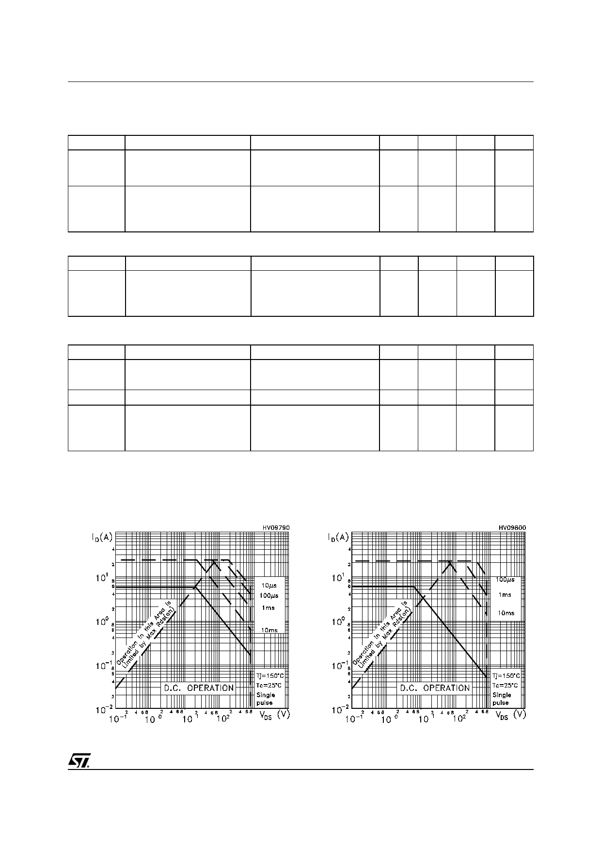
Safe Operating Area for TO-220
Safe Operating Area for TO-220FP
3/9
Share Link: 