STU36NB20 데이터 시트보기 (PDF) - STMicroelectronics
부품명
상세내역
제조사
STU36NB20 Datasheet PDF : 6 Pages
| |||
STU36NB20
N-CHANNEL ENHANCEMENT MODE
PowerMESH™ MOSFET
TYPE
STU36NB20
V DSS
200 V
RDS(on)
< 0.065 Ω
ID
36 A
PRELIMINARY DATA
s TYPICAL RDS(on) = 0.052 Ω
s EXTREMELY HIGH dv/dt CAPABILITY
s 100% AVALANCHE TESTED
s VERY LOW INTRINSIC CAPACITANCES
s GATE CHARGE MINIMIZED
s ± 30V GATE TO SOURCE VOLTAGE RATING
DESCRIPTION
Using the latest high voltage MESH OVERLAY™
process, SGS-Thomson has designed an
advanced family of power MOSFETs with
outstanding performances. The new patent
pending strip layout coupled with the Company’s
proprietary edge termination structure, gives the
lowest RDS(on) per area, exceptional avalanche
and dv/dt capabilities and unrivalled gate charge
and switching characteristics.
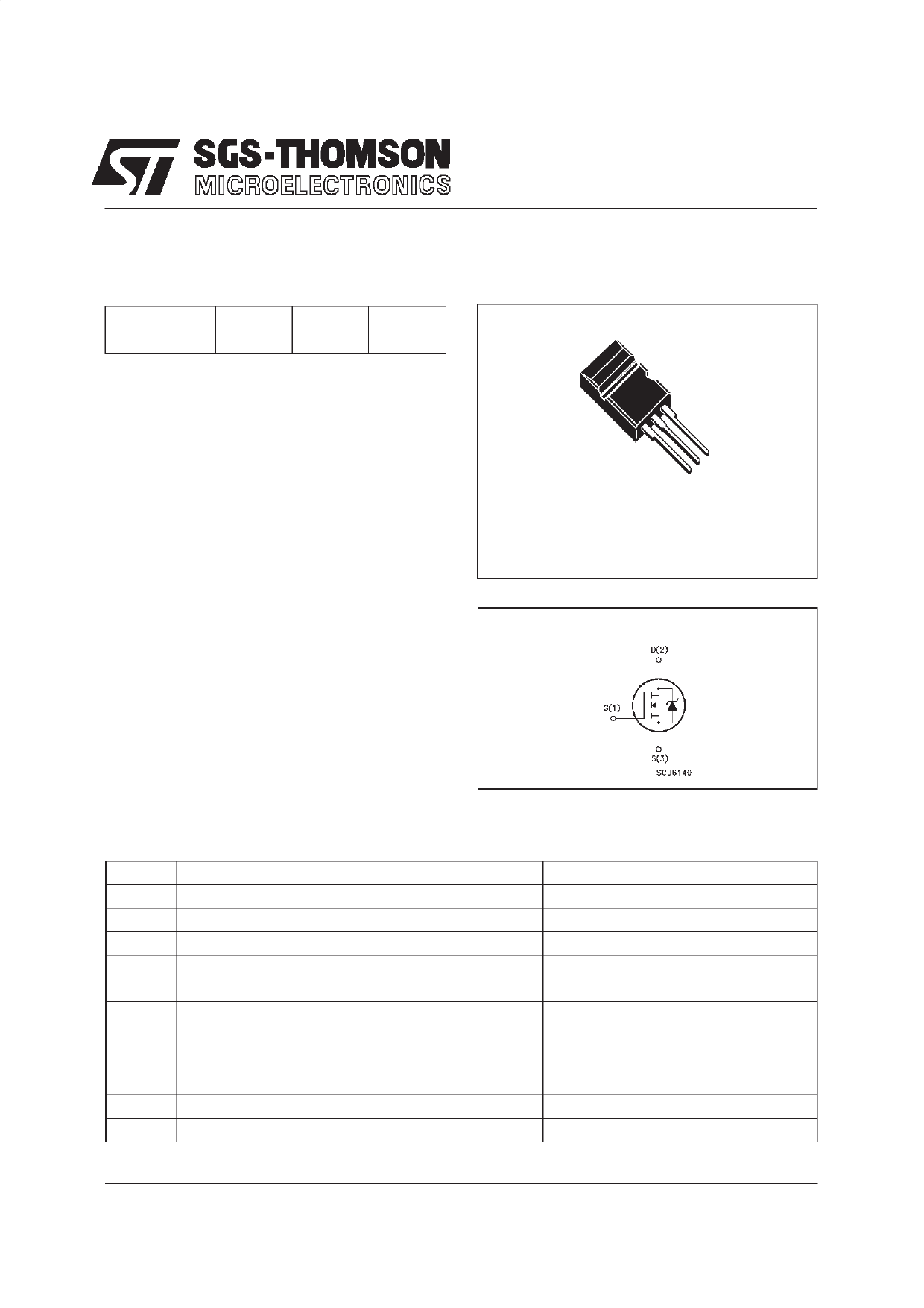
23
1
Max220
INTERNAL SCHEMATIC DIAGRAM
APPLICATIONS
s SWITCH MODE POWER SUPPLIES (SMPS)
s DC-AC CONVERTERS FOR WELDING
EQUIPMENT AND UNINTERRUPTIBLE
POWER SUPPLIES AND MOTOR DRIVE
ABSOLUTE MAXIMUM RATINGS
Symbol
Parameter
Value
Uni t
VDS
VDGR
VGS
ID
ID
IDM ( •)
Ptot
Drain-source Voltage (VGS = 0)
Drain- gate Voltage (RGS = 20 kΩ)
Gate-source Voltage
Drain Current (continuous) at Tc = 25 oC
Drain Current (continuous) at Tc = 100 oC
Drain Current (pulsed)
Tot al Dissipation at Tc = 25 oC
Derating Factor
200
200
± 30
36
23
144
160
1.28
V
V
V
A
A
A
W
W/oC
dv/dt(1) Peak Diode Recovery voltage slope
Tstg Storage Temperature
Tj
Max. Operating Junction Temperature
(•) Pulse width limited by safe operating area
5.5
-65 to 150
150
(1) ISD ≤36A, di/dt ≤ 200 A/µs, VDD ≤ V(BR)DSS, Tj ≤ TJMAX
V/ ns
oC
oC
January 1998
1/6
This is preliminary information on a new product now in development or undergoing evaluation. Details are subject to change without notice.
Share Link: 