SC9256S 데이터 시트보기 (PDF) - Silan Microelectronics
부품명
상세내역
제조사
SC9256S Datasheet PDF : 24 Pages
| |||
Silan
Semiconductors
SC9256
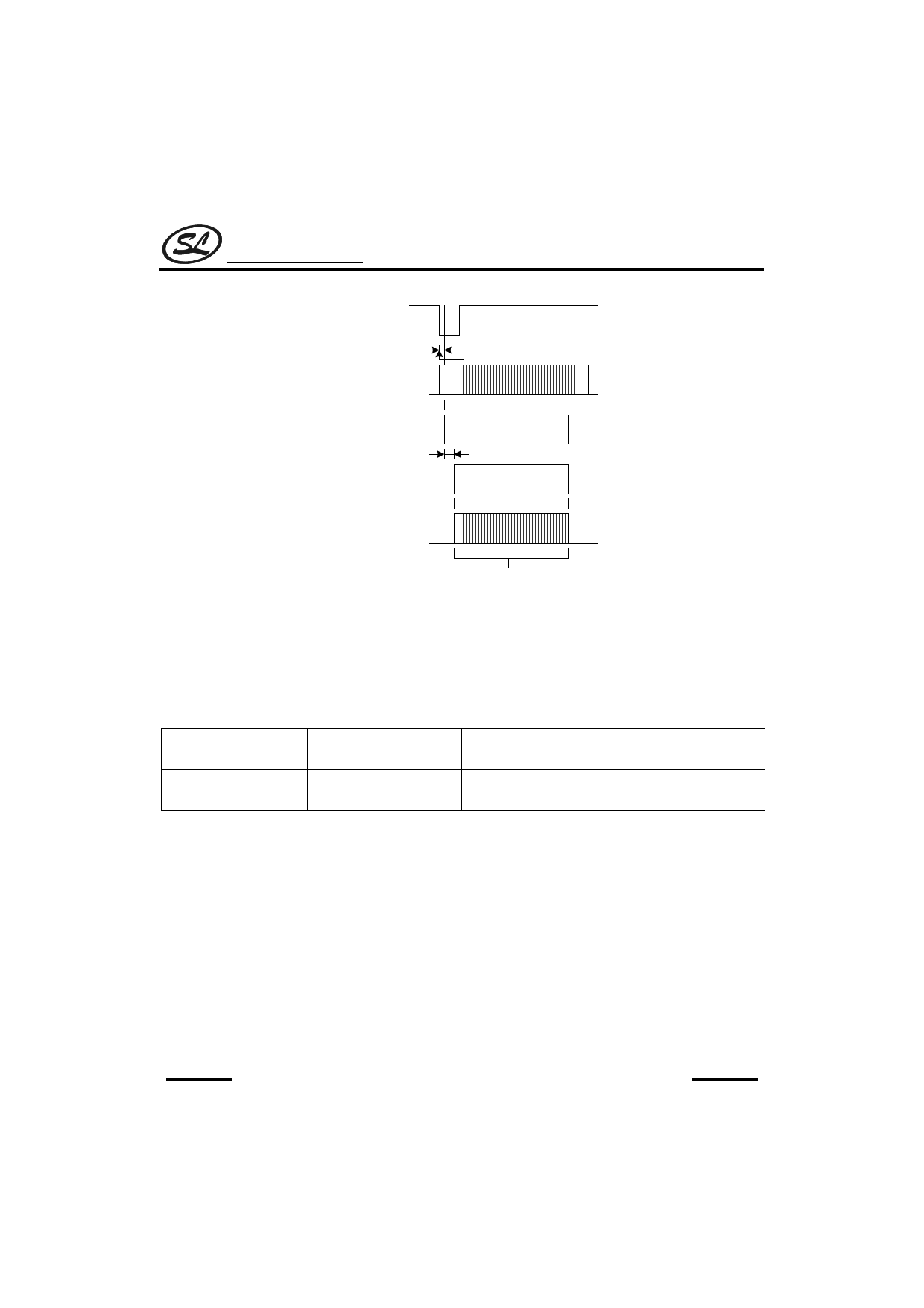
PERIOD
End
T1
IFIN1 OR
IFIN2
START bit set to "1"
BUSY bit
T2
Gate
Binary
counter
input
Clock pulse to be measured
Frequency measurement timing chart
0<T1≤0.25(µs), 0<T2 ≤1 (ms)
Note: 1. IFIN1 and IFIN2 input have built-in amps. Data are input by capacitor coupling. FMIN and AMIN operate at
low amplitude.
General-purpose I/O ports
These LSIs feature general-purpose output and I/O ports which are controlled through the serial ports.
Input/output form
port
Input/output configuration
Output port
Dedicated: 4 ports
N channel open-drain output
I/O ports
Dedicated: 1 port,
CMOS input/output
Maximum: 5 ports
1. General-purpose output ports (OT-1~OT-4)
Pins OT-1~OT-4 are general-purpose dedicated output ports. They have such uses as control signal output.
They are configured for N channel open-drain output and have an off withstanding voltage of 12V.
The data set in bits O1~O4 of the input register (D2H) are output in parallel from their correspond dedicated
output port pins OT-1~OT-4. SC9256 do not have dedicated output port OT-4, but setting the input register
(D2H) CLK (O4C) bit to “1” converts pin DO2 into output port OT-4 (configured for CMOS output).
The data set in bits O1~O4 of the input register (D2H) can also be read from the DATA pins as output register
(D3H) serial data O1~O4.
HANGZHOU SILAN MICROELECTRONICS JOINT-STOCK CO.,LTD
REV: 1.0
14
2002.01.30.
Share Link: 