CXD1185CQ 데이터 시트보기 (PDF) - Sony Semiconductor
부품명
상세내역
제조사
CXD1185CQ Datasheet PDF : 35 Pages
| |||
CXD1185CQ/CR
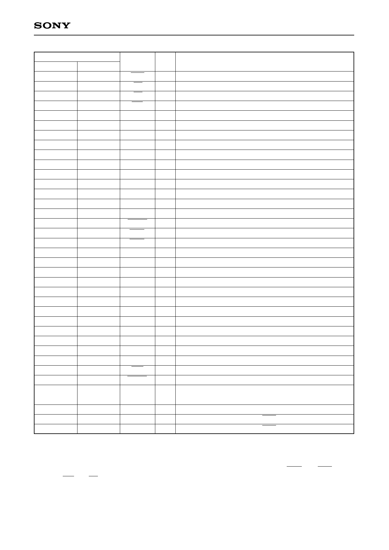
Pin No.
Symbol I/O
CXD1185CQ CXD1185CR
29
27
RES
I
30
28
CS
I
31
29
RE
I
32
30
WE
I
33
31
C7
I/O
34
32
C6
I/O
35
33
C5
I/O
36
34
C4
I/O
37
35
C3
I/O
38
36
C2
I/O
39
37
C1
I/O
40
38
C0
I/O
41
39
VSS
42
40
IRQ
O
43
41
DRQ
O
44
42
DACK
I
45
43
WED
I
46
44
RED
I
47
45
D0
I/O
48
46
D1
I/O
49
47
D2
I/O
50
48
D3
I/O
51
49
D4
I/O
52
50
D5
I/O
53
51
D6
I/O
54
52
D7
I/O
55
53
DP
I/O
56
54
VSS
57
55
CLK
I
58
56
VDD
59
57
INIT
O
60
58
TARG O
61
59
P0 (DOE) I/O
62
60
P1 (ARB) I/O
63
61
P2 (BSYO) I/O
64
62
P3 (SELO) I/O
Description
Reset all registers, negative logic
Chip select signal, negative logic
Internal register read signal, negative logic
Internal register write signal, negative logic
CPU bus bit 7
CPU bus bit 6
CPU bus bit 5
CPU bus bit 4
CPU bus bit 3
CPU bus bit 2
CPU bus bit 1
CPU bus bit 0
GND <note1>
Interrupt request signal
DMA request signal
DMA acknowledge signal, negative logic
Data bus write signal, negative logic <note3>
Data bus read signal, negative logic <note3>
Data bus bit 0 <note3>
Data bus bit 1 <note3>
Data bus bit 2 <note3>
Data bus bit 3 <note3>
Data bus bit 4 <note3>
Data bus bit 5 <note3>
Data bus bit 6 <note3>
Data bus bit 7 <note3>
Data bus parity signal <note4>
GND <note1>
Clock input, 5 –16 MHz
+5 V <note1>
Initiator operation indicator signal
Target operation indicator signal
General-use port bit 0 (SCSI data output authorization)
<note2>
General-use port bit 1 (arbitration in progress) <note2>
General-use port bit 2 (SCSI BSY output)
<note2>
General-use port bit 3 (SCSI SEL output)
<note2>
<Note1> All VDD and VSS pins should be connected to the power supply and ground, respectively.
<Note2> Items in parentheses ( ) indicate the meaning of the signal when operating in the SCSI differential
mode.
<Note3> In systems where the CPU and data buses are not separate, connect the WED and RED pins to
WE and RE, respectively, and Pins D7-D0 to Pins C7-C0.
<Note4> If the data bus parity signal is not used, pull up the DP pin using a resistor.
—5—
Share Link: 