AD9830 데이터 시트보기 (PDF) - Analog Devices
부품명
상세내역
제조사
AD9830 Datasheet PDF : 16 Pages
| |||
AD9830
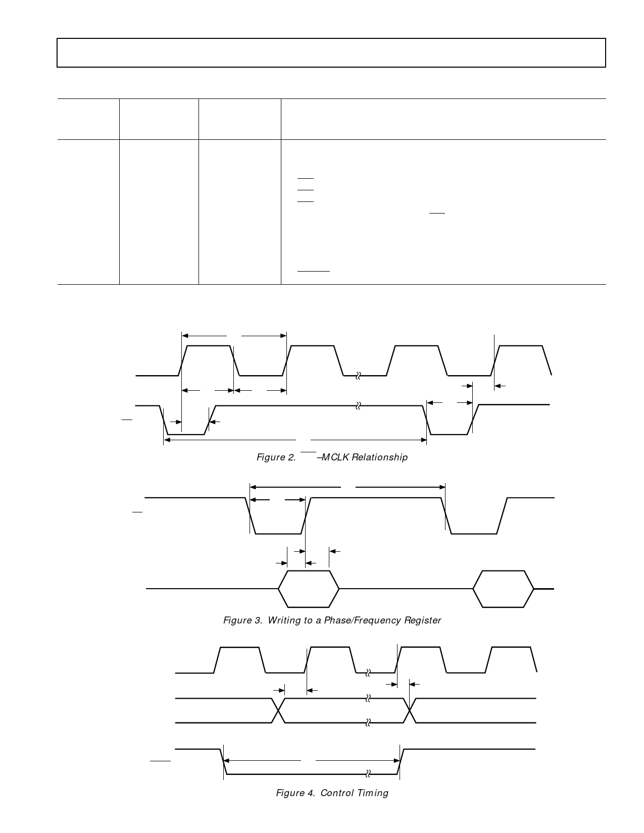
TIMING CHARACTERISTICS (VDD = +5 V ؎ 5%; AGND = DGND = 0 V, unless otherwise noted)
Parameter
Limit at
TMIN to TMAX
(A Version)
Units
Test Conditions/Comments
t1
20
t2
8
t3
8
t41
8
t4A1
8
t5
8
t6
t1
t7
5
t8
3
t91
8
t9A1
8
t10
t1
ns min
ns min
ns min
ns min
ns min
ns min
ns min
ns min
ns min
ns min
ns min
ns min
NOTES
1See Pin Description section.
Guaranteed by design, but not production tested.
MCLK Period
MCLK High Duration
MCLK Low Duration
WR Rising Edge Before MCLK Rising Edge
WR Rising Edge After MCLK Rising Edge
WR Pulse Width
Duration Between Consecutive WR Pulses
Data/Address Setup Time
Data/Address Hold Time
FSELECT, PSEL0, PSEL1 Setup Time Before MCLK Rising Edge
FSELECT, PSEL0, PSEL1 Setup Time After MCLK Rising Edge
RESET Pulse Duration
t1
MCLK
t2
t3
t4
t5
WR
t4A
t6
Figure 2. WR–MCLK Relationship
t6
t5
WR
A0, A1, A2
DATA
t8
t7
VALID DATA
Figure 3. Writing to a Phase/Frequency Register
VALID DATA
MCLK
FSELECT
PSEL0, PSEL1
VALID DATA
t9
VALID DATA
t9A
VALID DATA
REV. A
RESET
t10
Figure 4. Control Timing
–3–
Share Link: 