SG1525A 데이터 시트보기 (PDF) - Microsemi Corporation
부품명
상세내역
제조사
SG1525A Datasheet PDF : 13 Pages
| |||
SG1525A/SG2525A/SG3525A
SG1527A/SG2527A/SG3527A
Regulating Pulse Width Modulator
Description
The SG1525A/1527A series of pulse width modulator integrated
circuits are designed to offer improved performance and lower
external parts count when used to implement all types of switching
power supplies. The on-chip +5.1 V reference is trimmed to ±1%
initial accuracy and the input common-mode range of the error
amplifier includes the reference voltage, eliminating external
potentiometers and divider resistors. A Sync input to the oscillator
allows multiple units to be slaved together, or a single unit to be
synchronized to an external system clock. A single resistor between
the CT pin and the Discharge pin provides a wide range of deadtime
adjustment. These devices also feature built-in soft-start circuitry
with only a timing capacitor required externally. A Shutdown pin
controls both the soft-start circuitry and the output stages, providing
instantaneous turn-off with soft-start recycle for slow turn-on. These
functions are also controlled by an undervoltage lockout which
keeps the outputs off and the soft-start capacitor discharged for
input voltages less than that required for normal operation. Another
unique feature of these PWM circuits is a latch following the
comparator. Once a PWM pulse has been terminated for any
reason, the outputs remain off for the duration of the period. The
latch is reset with each clock pulse. The output stages are totem-
pole designs capable of sourcing or sinking in excess of 200mA.
The SG1525A output stage features NOR logic, giving a LOW
output for an OFF state. The SG1527A utilizes OR logic, which
results in a HIGH output level when OFF.
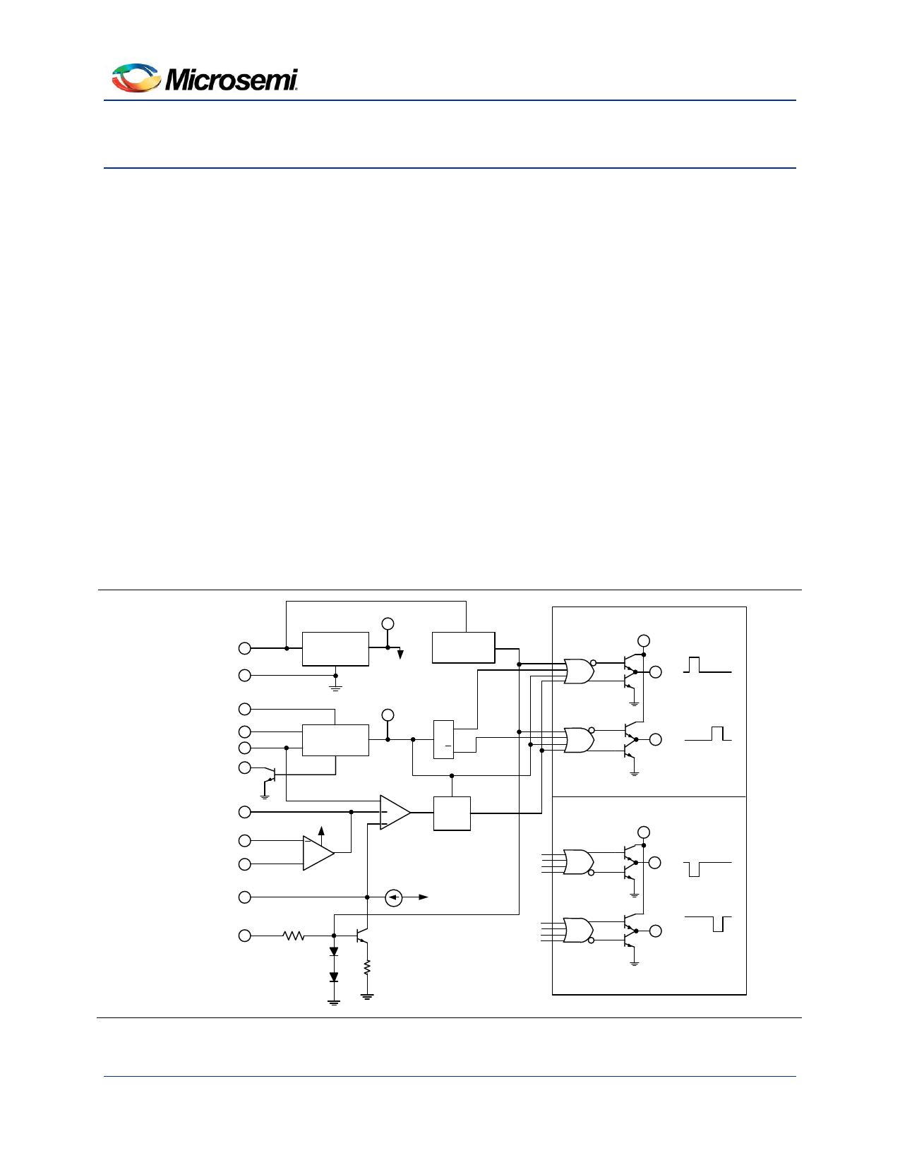
Block Diagram
Features
8V to 35V Operation
5.1V Reference Trimmed to 1%
100Hz to 500kHz Oscillator Range
Separate Oscillator Sync Terminal
Adjustable Deadtime Control
Internal Soft-start
Input Undervoltage Lockout
Latching P.W.M. to Prevent Multiple Pulses
Dual Source/Sink Output Drivers
High Reliability Features
Following are the high reliability features of SG1525A
and SG1527A:
Available to MIL-STD-883, ¶ 1.2.1
MIL-M38510/12602BEA - JAN1525AJ
MIL-M38510/12604BEA - JAN1527AJ
MSC-AMS level “S” Processing Available
+VIN
GROUND
SYNC
RT
CT
DISCHARGE
COMPENSATION
INV. INPUT
N.I. INPUT
SOFT-SART
SHUTDOWN
VREF
REFERENCE
REGULATOR
U.V.
LOCKOUT
TO
INTERNAL CIRCUITRY
OSC OUTPUT
Q
OSCILLATOR
Q
F/F
P.W.M.
R
+
S
LATCH
VIN
+
ERROR
AMP
5k
50µA
VREF
5k
VC
OUTPUT A
OUTPUT B
SG1525A OUTPUT STAGE
VC
OUTPUT A
OUTPUT B
SG1527A OUTPUT STAGE
Figure 1 · Block Diagram
September 2014 Rev. 1.4a
www.microsemi.com
1
© 2014 Microsemi Corporation
Share Link: 