HAT2167H(2003) 데이터 시트보기 (PDF) - Renesas Electronics
부품명
상세내역
제조사
HAT2167H Datasheet PDF : 10 Pages
| |||
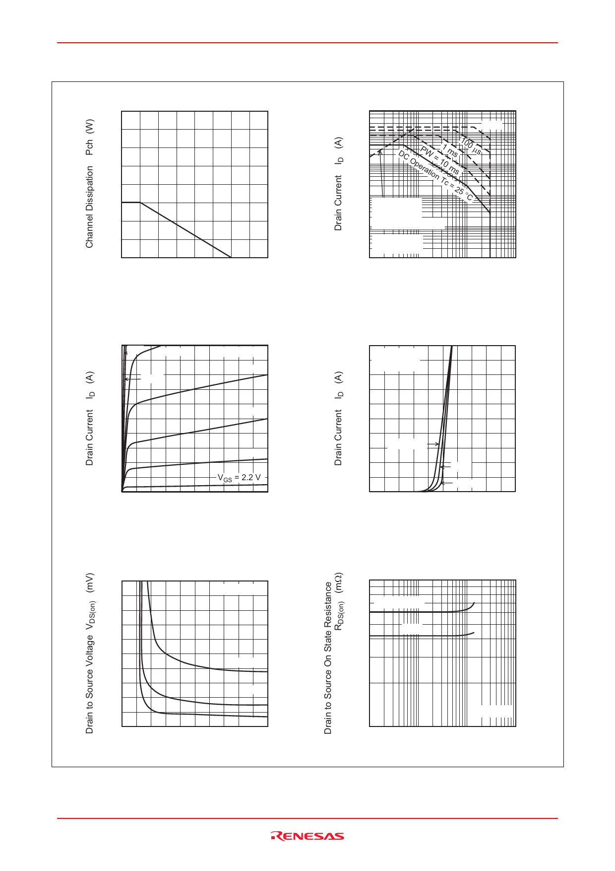
HAT2167H
Electrical Characteristics
(Ta = 25°C)
Item
Symbol Min
Drain to source breakdown voltage V(BR)DSS 30
Gate to source breakdown voltage V(BR)GSS ± 20
Gate to source leak current
IGSS
—
Zero gate voltage drain current
IDSS
—
Gate to source cutoff voltage
VGS(off) 1.0
Static drain to source on state
resistance
RDS(on) —
RDS(on) —
Forward transfer admittance
|yfs|
42
Input capacitance
Ciss —
Output capacitance
Coss —
Reverse transfer capacitance
Crss —
Gate resistance
Rg
—
Total gate charge
Qg
—
Gate to source charge
Qgs —
Gate to drain charge
Qgd —
Turn-on delay time
td(on)
—
Rise time
tr
—
Turn-off delay time
td(off)
—
Fall time
tf
—
Body–drain diode forward voltage VDF
—
Body–drain diode reverse recovery trr
—
time
Notes: 4. Pulse test
Typ Max
—
—
—
—
—
± 10
—
1
—
2.5
4.2 5.5
6.1 9.3
70
—
2700 —
620 —
200 —
0.5 —
17
—
8
—
3.7 —
11
—
30
—
45
—
6
—
0.85 1.10
30
—
Unit
V
V
µA
µA
V
mΩ
mΩ
S
pF
pF
pF
Ω
nc
nc
nc
ns
ns
ns
ns
V
ns
Test Conditions
ID = 10 mA, VGS = 0
IG = ±100 µA, VDS = 0
VGS = ±16 V, VDS = 0
VDS = 30 V, VGS = 0
VDS = 10 V, I D = 1 mA
ID = 20 A, VGS = 10 V Note4
ID = 20 A, VGS = 4.5 V Note4
ID = 20 A, VDS = 10 V Note4
VDS = 10 V
VGS = 0
f = 1 MHz
VDD = 10 V
VGS = 4.5 V
ID = 40 A
VGS = 10 V, ID = 20 A
VDD ≅ 10 V
RL = 0.5 Ω
Rg = 4.7 Ω
IF = 40 A, VGS = 0 Note4
IF = 40 A, VGS = 0
diF/ dt = 100 A/ µs
Rev.4.00, Jun.04.2003, page 3 of 10
Share Link: 