5962F9563501QXC 데이터 시트보기 (PDF) - Intersil
부품명
상세내역
제조사
5962F9563501QXC Datasheet PDF : 36 Pages
| |||
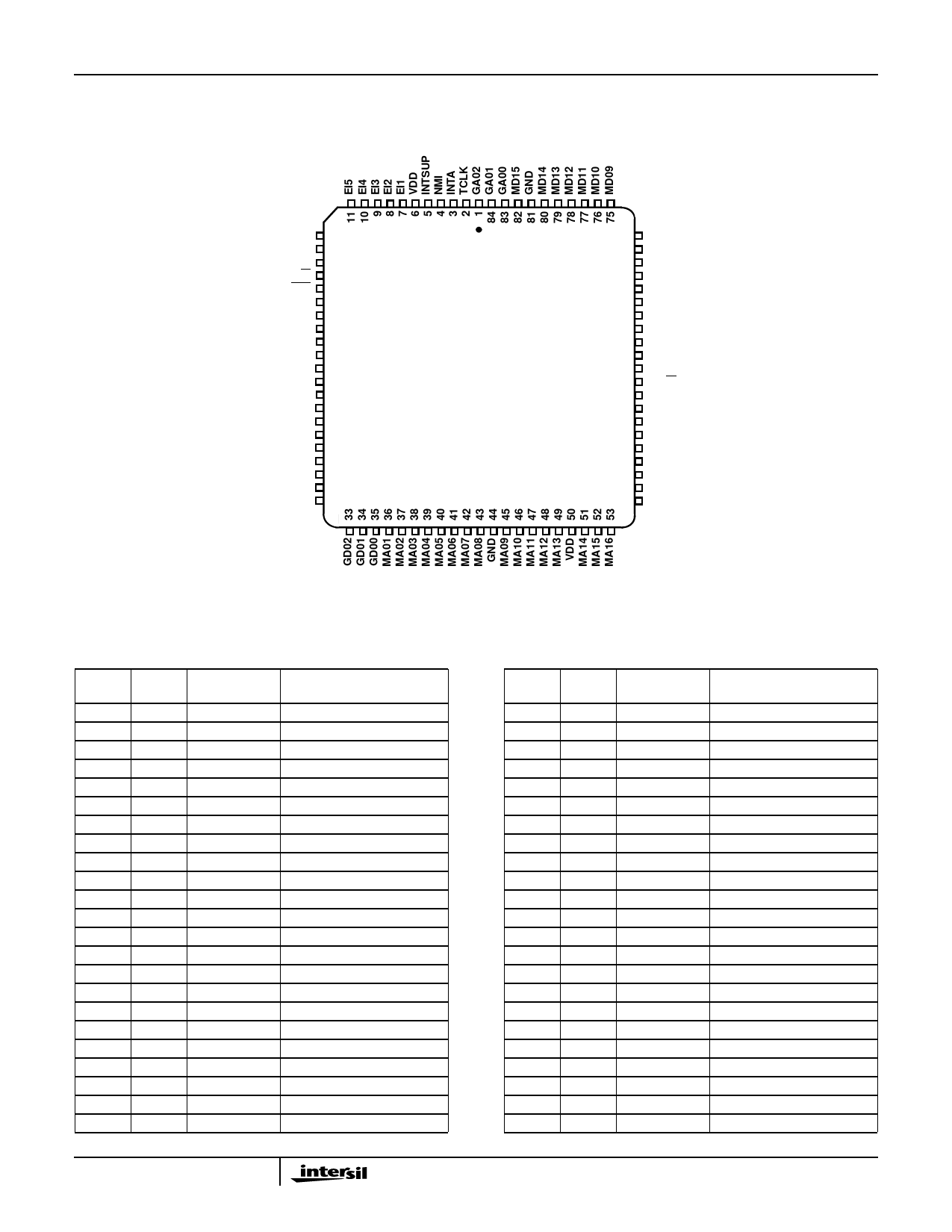
Pinouts (Continued)
HS-RTX2010RH
HS9-RTX2010RH
(LEAD LENGTH NOT TO SCALE) SEE INTERSIL OUTLINE R84.A
RESET 12
WAIT 13
ICLK 14
GR/W 15
GIO 16
GD15 17
GD14 18
GD13 19
GND 20
GD12 21
GD11 22
GD10 23
GD09 24
GD08 25
GD07 26
VDD 27
GD06 28
GD05 29
GD04 30
GD03 31
GND 32
HS-RTX2010RH
TOP VIEW
74 MD08
73 VDD
72 MD07
71 MD06
70 MD05
69 GND
68 MD04
67 MD03
66 MD02
65 MD01
64 MD00
63 MR/W
62 PCLK
61 BOOT
60 NEW
59 UDS
58 LDS
57 GND
56 MA19
55 MA18
54 MA17
NOTE: An overbar on a signal name represents an active LOW signal.
PGA And CQFP
Pin/Signal Assignments
CQFP
1
2
3
4
5
6
7
8
9
10
11
12
13
14
15
16
17
18
19
20
21
22
23
PGA
PIN
C6
A6
A5
B5
C5
A4
B4
A3
A2
B3
A1
B2
C2
B1
C1
D2
D1
E3
E2
E1
F2
F3
G3
SIGNAL
NAME
GA02
TCLK
INTA
NMI
INTSUP
VDD
EI1
EI2
EI3
EI4
EI5
RESET
WAIT
ICLK
GR/W
GIO
GD15
GD14
GD13
GND
GD12
GD11
GD10
TYPE
Output; Address Bus
Output
Output
Input
Input
Power
Input
Input
Input
Input
Input
Input
Input
Input
Output
Output
I/O; Data Bus
I/O; Data Bus
I/O; Data Bus
Ground
I/O; Data Bus
I/O; Data Bus
I/O; Data Bus
3
PGA And CQFP
Pin/Signal Assignments (Continued)
CQFP
24
25
26
27
28
29
30
31
32
33
34
35
36
37
38
39
40
41
42
43
44
45
46
PGA
PIN
G1
G2
F1
H1
H2
J1
K1
J2
L1
K2
K3
L2
L3
K4
L4
J5
K5
L5
K6
J6
J7
L7
K7
SIGNAL
NAME
GD09
GD08
GD07
VDD
GD06
GD05
GD04
GD03
GND
GD02
GD01
GD00
MA01
MA02
MA03
MA04
MA05
MA06
MA07
MA08
GND
MA09
MA10
TYPE
I/O; Data Bus
I/O; Data Bus
I/O; Data Bus
Power
I/O; Data Bus
I/O; Data Bus
I/O; Data Bus
I/O; Data Bus
Ground
I/O; Data Bus
I/O; Data Bus
I/O; Data Bus
Output; Address Bus
Output; Address Bus
Output; Address Bus
Output; Address Bus
Output; Address Bus
Output; Address Bus
Output; Address Bus
Output; Address Bus
Ground
Output; Address Bus
Output; Address Bus
Share Link: 