IMC020FLSA 데이터 시트보기 (PDF) - Intel
부품명
상세내역
제조사
IMC020FLSA Datasheet PDF : 39 Pages
| |||

SERIES 2 FLASH MEMORY CARDS
ADDRESS
4100H
BIT 7
ADM
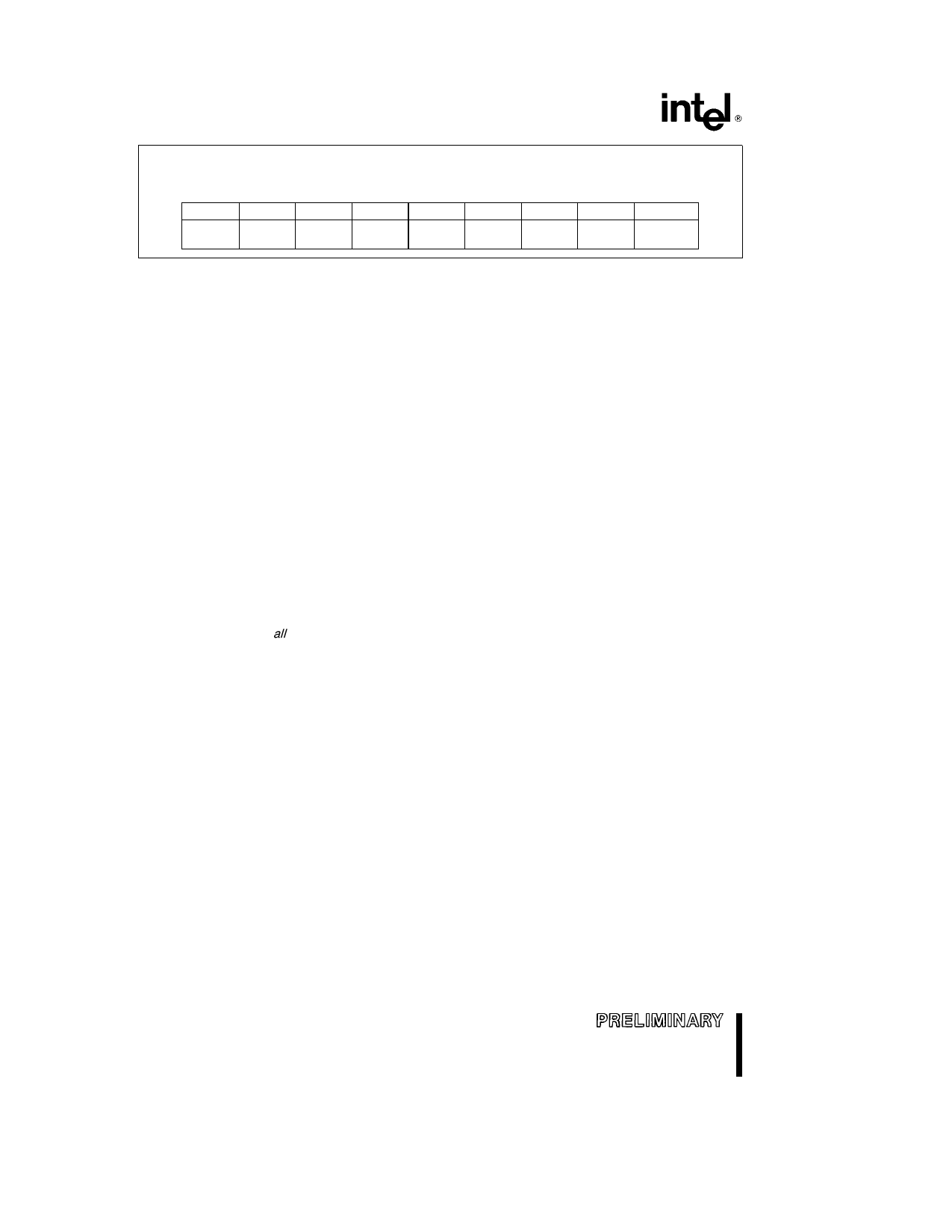
CARD STATUS REGISTER
(Read Only Register)
BIT 6
ADS
BIT 5
SRESET
BIT 4
CMWP
BIT 3
RP
BIT 2
CISWP
BIT 1
WP
BIT 0
RDY BSY
Figure 7 CARD STATUS REGISTER (Intel) Provides a Quick Review of the Card’s Status
CARD STATUS REGISTER (INTEL)
The Read-Only CARD STATUS REGISTER (Attri-
bute Memory Plane Address 4100H Figure 7) re-
turns generalized status of the Series 2 Card and its
CMRs
Bit 0 (RDY BSY ) reflects the card’s RDY BSY
(Ready-Busy) output Software polling of this bit pro-
vides data-write or block-erase operation status A
zero indicates a busy device(s) in the card
Bit 1 (WP) reports the position of the card’s Write
Protection switch with 1 indicating write protected It
reports the status of the WP pin
Bit 2 (CISWP) reflects whether the Common Memo-
ry CIS is write protected using the WRITE PROTECT
REGISTER with 1 indicating write protected
Bit 3 (RP) reports whether the entire flash memory
array is in ‘‘Deep-Sleep’’ (Reset-PwrDwn) mode
with 1 indicating ‘‘Deep-Sleep’’ This bit reflects the
RP bit of the GLOBAL RESET-POWERDOWN REG-
ISTER Powering down all device pairs individually
(using the Sleep Control Register) also sets this bit
Bit 4 (CMWP) reports whether the Common Memory
Plane (minus Common Memory CIS) is write protect-
ed via the WRITE PROTECT REGISTER with 1 indi-
cating write protected
Bit 5 (SRESET) reflects the SRESET bit of the SOFT
RESET REGISTER It reports that the card is in Soft
Reset with 1 indicating reset When this bit is zero
the flash memory array and CMRs may be ac-
cessed otherwise clear it via the SRESET REGIS-
TER
Bit 6 (ADS ANY DEVICE SLEEP) is the ‘‘ORed’’
value of the SLEEP CONTROL REGISTER Power-
ing down any device pair sets this bit
Bit 7 (ADM ANY DEVICE MASKED) is the ‘‘ORed’’
value of the READY BUSY MASK REGISTER
Masking any device sets this bit
WRITE PROTECTION REGISTER
(INTEL)
The WRITE PROTECTION REGISTER (Attribute
Memory Plane Address 4104H Figure 8) selects
whether the optional Common Memory CIS and the
remaining Common Memory blocks are write pro-
tected (see Figure 4)
Enable Common Memory CIS write protection by
writing a 1 to the CISWP Bit (bit 0)
Enable write protection of the remaining Common
Memory blocks by writing a 1 to the CMWP Bit (bit
1)
In the power-on default state both bits are 0 and
therefore not write protected
Reserved bits (2 – 7) have undefined values and
should be written as zeroes for future compatibility
12