IMC020FLSA 데이터 시트보기 (PDF) - Intel
부품명
상세내역
제조사
IMC020FLSA Datasheet PDF : 39 Pages
| |||
SERIES 2 FLASH MEMORY CARDS
If the READY-BUSY MASK REGISTER bits are set
to ones (masked condition) the RDY BSY output
and the CARD STATUS REGISTER RDY BSY bit
will reflect a READY condition regardless of the
state of the corresponding devices The READY-
BUSY MASK REGISTER does not affect the
READY-BUSY STATUS REGISTER allowing soft-
ware polling to determine operation status
Unmasked is the default condition for the bits in this
register On memory cards with fewer than 20 devic-
es unused device mask bits appear as masked
READY-BUSY MODE REGISTER
(INTEL)
The READY-BUSY MODE REGISTER (Attribute
Memory Plane Address 4140H Figure 12) provides
the selection of two types of system interfacing for
the busy-to-ready transition of the card’s
RDY BSY pin
1 The standard PCMCIA READY-BUSY MODE in
which the card’s RDY BSY signal generates a
low-to-high transition (from busy to ready) only
after all busy devices (not including masked
devices) have completed their data-write or block-
erase operations This may result in a long inter-
rupt latency
2 A High-Performance mode that generates a low-
to-high (from busy-to-ready) transition after each
device becomes ready This provides the host
system with immediate notification that a specific
device’s operation has completed and that de-
vice may now be used This is particularly useful
in a file management application where a block
pair containing only deleted files is being erased
to free up space so new file data may be written
Enabling the HIGH-PERFORMANCE READY-BUSY
MODE requires a three step sequence
1 Set all bits in the READY BUSY MASK REGIS-
TER This prevents ready devices from triggering
an unwanted interrupt when step 3 is performed
2 Write 01H to the READY-BUSY MODE REGIS-
TER This sets the MODE bit
3 Write 01H to the READY-BUSY MODE REGIS-
TER This clears the RACK bit
The MODE and RACK bits must be written in the
prescribed sequence not simultaneously The
card’s circuitry is designed purposely in this manner
to prevent an initial unwanted busy-to-ready tran-
sition Note that in Step 2 writing to the RACK bit is
a Don’t Care
When the High-Performance Mode is enabled spe-
cific READY-BUSY MASK bits must be cleared after
an operation is initiated on the respective devices
After each device becomes ready the RDY BSY
pin makes a low-to-high transition To catch the next
device’s completion of an operation the RACK bit
must be cleared by writing ‘‘01H’’ to the Ready Busy
Mode Register
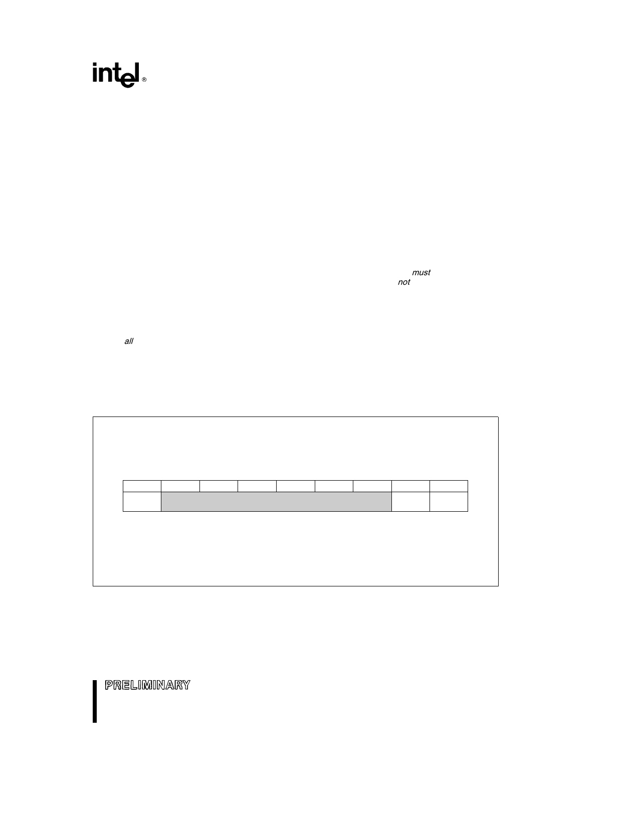
ADDRESS
4140H
BIT 7
READY-BUSY MODE REGISTER
(Read Write Register)
BIT 6
BIT 5
BIT 4
BIT 3
RESERVED FOR FUTURE USE
BIT 2
BIT 1
RACK
BIT 0
MODE
MODE e READY-BUSY MODE
0 e PCMCIA MODE
1 e HIGH PERFORMANCE
RACK e READY ACKNOWLEDGE CLEAR TO
SET UP RDY BSY PIN THEN CLEAR AFTER
EACH DEVICE BECOMES READY TO ACKNOWL-
EDGE TRANSITION
Figure 12 High Performance Ready-Busy Mode REGISTER (Intel)
Used to Trigger a Ready Interrupt for Each Device
15
Share Link: 