OR4E10 데이터 시트보기 (PDF) - Agere -> LSI Corporation
부품명
상세내역
제조사
OR4E10 Datasheet PDF : 124 Pages
| |||
Preliminary Data Sheet
December 2000
Programmable Logic Cells (continued)
WD[7:0]
8
4
PLC
4
PLC
WD[7:4]
5 WA RA 5
WPE 1
WPE 2
WE
RD[7:4]
WD[3:0]
5 WA RA 5
WPE 1
WPE 2
WE
RD[3:0]
ORCA Series 4 FPGAs
4
PLC
4
PLC
WD[7:4]
5 WA RA 5
WPE 1
WPE 2
WE
RD[7:4]
WD[3:0]
5 WA RA 5
WPE 1
WPE 2
WE
RD[3:0]
RD[7:0] 8
WE
WA[6:0] 7
RA[6:0] 7
CLK
RE
RE
4
RE
4
RE
4
RE
4
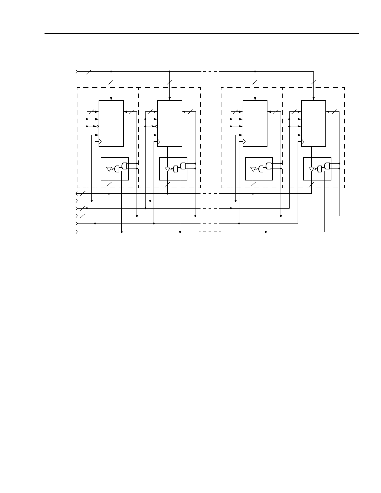
Figure 13. Memory Mode Expansion Example—128 x 8 RAM
5-5749(F)
Supplemental Logic and Interconnect Cell
Each PLC contains a SLIC embedded within the PLC
routing, outside of the PFU. As its name indicates, the
SLIC performs both logic and interconnect (routing)
functions. Its main features are 3-statable, bidirectional
buffers, and a PAL-like decoder capability. Figure 14
shows a diagram of a SLIC with all of its features
shown. All modes of the SLIC are not available at one
time.
The ten SLIC inputs can be sourced directly from the
PFU or from the general routing fabric. SI[0:9] inputs
can come from the horizontal or vertical routing, and
I[0:9} comes from the PFU outputs O[9:0]. These
inputs can also be tied to a logical 1 or 0 constant. The
inputs are twin-quad in nature and are segregated into
two groups of four nibbles and a third group of two
inputs for control. Each input nibble groups also have
3-state capability; however, the third pair does not.
There is one 3-state control (TRI) for each SLIC, with
the capability to invert or disable the 3-state control for
each group of four BIDIs. Separate 3-state control for
each nibblewide group is achievable by using the
SLICs decoder (DEC) output, driven by the group of
two BIDIs, to control the 3-state of one BIDI nibble
while using the TRI signal to control the 3-state of the
other BIDI nibble. Figure 15 shows the SLIC in buffer
mode with available 3-state control from the TRI and
DEC signals. If the entire SLIC is acting in a buffer
capacity, the DEC output may be used to generate a
constant logic 1 (VHI) or logic 0 (VLO) signal for general
use.
The SLIC may also be used to generate PAL-like AND-
OR with optional INVERT (AOI) functions or a decoder
of up to 10 bits. Each group of buffers can feed into an
AND gate (4-input AND for the nibble groups and
2-input AND for the other two buffers). These AND
gates then feed into a 3-input gate that can be config-
ured as either an AND gate or an OR gate. The output
of the 3-input gate is invertible and is output at the DEC
output of the SLIC. Figure 19 shows the SLIC in full
decoder mode.
The functionality of the SLIC is parsed by the two
nibblewide groups and the 2-bit buffer group. Each of
these groups may operate independently as BIDI buff-
ers (with or without 3-state capability for the nibblewide
groups) or as a PAL/decoder.
Lucent Technologies Inc.
21
Share Link: 