29104BJA 데이터 시트보기 (PDF) - Intersil
부품명
상세내역
제조사
29104BJA Datasheet PDF : 7 Pages
| |||
HM-65162
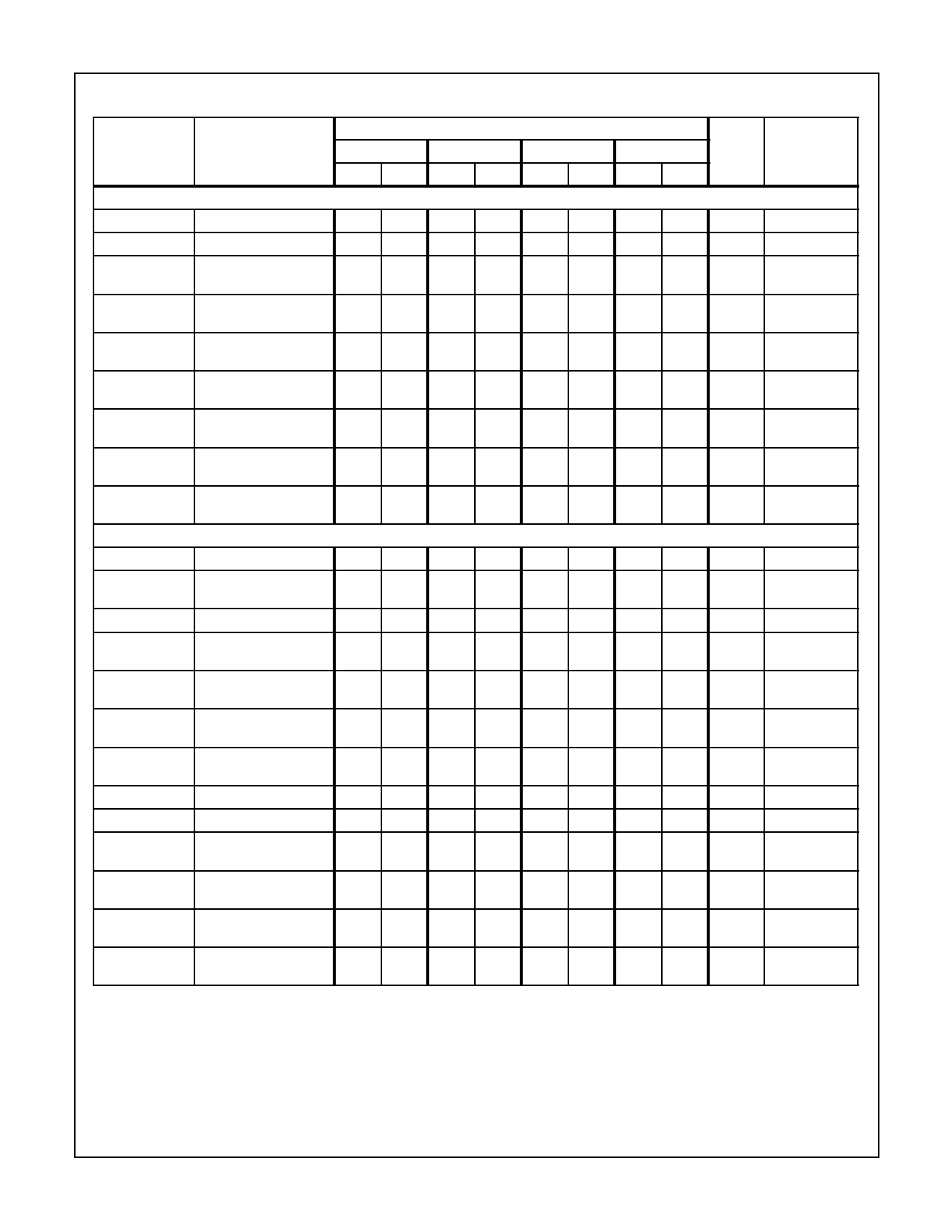
AC Electrical Specifications VCC = 5V ±10%, TA = -40oC to +85oC (HM-65162S-9, HM-65162B-9, HM65162-9, HM-65162C-9)
LIMITS
HM-65162S-9 HM-65162B-9 HM-65162-9 HM-65162C-9
SYMBOL
PARAMETER
MIN MAX MIN MAX MIN MAX MIN MAX UNITS CONDITIONS
READ CYCLE
(1) TAVAX Read Cycle Time
55
-
70
-
90
-
90
-
ns
(Notes 1, 3)
(2) TAVQV Address Access Time
-
55
-
70
-
90
-
90
ns (Notes 1, 3, 4)
(3) TELQV
Chip Enable Access
Time
-
55
-
70
-
90
-
90
ns
(Notes 1, 3)
(4) TELQX
Chip Enable Output
Enable Time
5
-
5
-
5
-
5
-
ns
(Notes 2, 3)
(5) TGLQV Output Enable Access
-
35
-
50
-
65
-
65
ns
(Notes 1, 3)
Time
(6) TGLQX Output Enable Output
5
-
5
-
5
-
5
-
ns
(Notes 2, 3)
Enable Time
(7) TEHQZ
Chip Enable Output
Disable Time
-
35
-
35
-
50
-
50
ns
(Notes 2, 3)
(8) TGHQZ Output Enable Output
-
30
-
35
-
40
-
40
ns
(Notes 2, 3)
Disable Time
(9) TAVQX
Output Hold From
Address Change
5
-
5
-
5
-
5
-
ns
(Notes 1, 3)
WRITE CYCLE
(10) TAVAX Write Cycle Time
55
-
70
-
90
-
90
-
ns
(Notes 1, 3)
(11) TELWH Chip Selection to End of 45
-
45
-
55
-
55
-
Write
ns
(Notes 1, 3)
(12) TAVWL Address Setup Time
5
-
10
-
10
-
10
-
ns
(Notes 1, 3)
(13) TWLWH Write Enable Pulse
Width
40
-
40
-
55
-
55
-
ns
(Notes 1, 3)
(14) TWHAX Write Enable Read
Setup Time
10
-
10
-
10
-
10
-
ns
(Notes 1, 3)
(15) TGHQZ Output Enable Output
-
30
-
35
-
40
-
40
ns
(Notes 2, 3)
Disable Time
(16) TWLQZ
Write Enable Output
Disable Time
-
30
-
40
-
50
-
50
ns
(Notes 2, 3)
(17) TDVWH Data Setup Time
25
-
30
-
30
-
30
-
ns
(Notes 1, 3)
(18) TWHDX Data Hold Time
10
-
10
-
15
-
15
-
ns
(Notes 1, 3)
(19) TWHQX Write Enable Output
Enable Time
0
-
0
-
0
-
0
-
ns
(Notes 1, 3)
(20) TWLEH Write Enable Pulse
Setup Time
45
-
40
-
55
-
55
-
ns
(Notes 1, 3)
(21) TDVEH
Chip Enable Data
Setup Time
25
-
30
-
30
-
30
-
ns
(Notes 1, 3)
(22) TAVWH Address Valid to End of 45
-
50
-
65
-
65
-
Write
ns
(Notes 1, 3)
NOTES:
1. Input pulse levels: 0 to 3.0V; Input rise and fall times: 5ns (max); Input and output timing reference level: 1.5V; Output load: 1 TTL gate
equivalent and CL = 50pF (min) - for CL greater than 50pF, access time is derated by 0.15ns per pF.
2. Tested at initial design and after major design changes.
3. VCC = 4.5 and 5.5V.
4. TAVQV = TELQV + TAVEL.
4
Share Link: 