5962-9089401MEA 데이터 시트보기 (PDF) - Analog Devices
부품명
상세내역
제조사
5962-9089401MEA Datasheet PDF : 14 Pages
| |||
OFFSET NULLING
Input voltage offset nulling of the AD526 is best accomplished
at a gain of 16, since the referred-to-input (RTI) offset is ampli-
fied the most at this gain and therefore is most easily trimmed.
The resulting trimmed value of RTI voltage offset typically
varies less than 3 µV across all gain ranges.
Note that the low input current of the AD526 minimizes RTI
voltage offsets due to source resistance.
+VS
0.1F
16 15 14 13 12 11 10
A1 A0 CS CLK A2 B
LOGIC AND LATCHES
OUT
9 FORCE
16 8 4 2 1
GAIN NETWORK
–
AD526
+
VOUT
1 2 3 4 5 6 7 8 OUT
SENSE
VIN
20k⍀
0.1F
–VS
Figure 39. Offset Voltage Null Circuit
OUTPUT CURRENT BOOSTER
The AD526 is rated for a full ± 10 V output voltage swing into
2 kΩ. In some applications, the need exists to drive more cur-
rent into heavier loads. As shown in Figure 40, a high current
booster may be connected “inside the loop” of the SPGA to
provide the required current boost without significantly degrad-
ing overall performance. Nonlinearities, offset and gain inaccu-
racies of the buffer are minimized by the loop gain of the
AD526 output amplifier.
+VS
0.1F
16 15 14 13 12 11 10
A1 A0 CS CLK A2 B
LOGIC AND LATCHES
16 8 4 2 1
OUT
9 FORCE
GAIN NETWORK
–
AD526
+
1 2 3 4 5 6 7 8 OUT
SENSE
0.1F
VIN
–VS
0.01F
HOS-100
0.01F
RL
AD526
CASCADED OPERATION
A cascade of two AD526s can be used to achieve binarily
weighted gains from 1 to 256. If gains from 1 to 128 are needed,
no additional components are required. This is accomplished by
using the B pin as shown in Figure 38. When the B pin is low,
the AD526 is held in a unity gain stage independent of the other
gain code values.
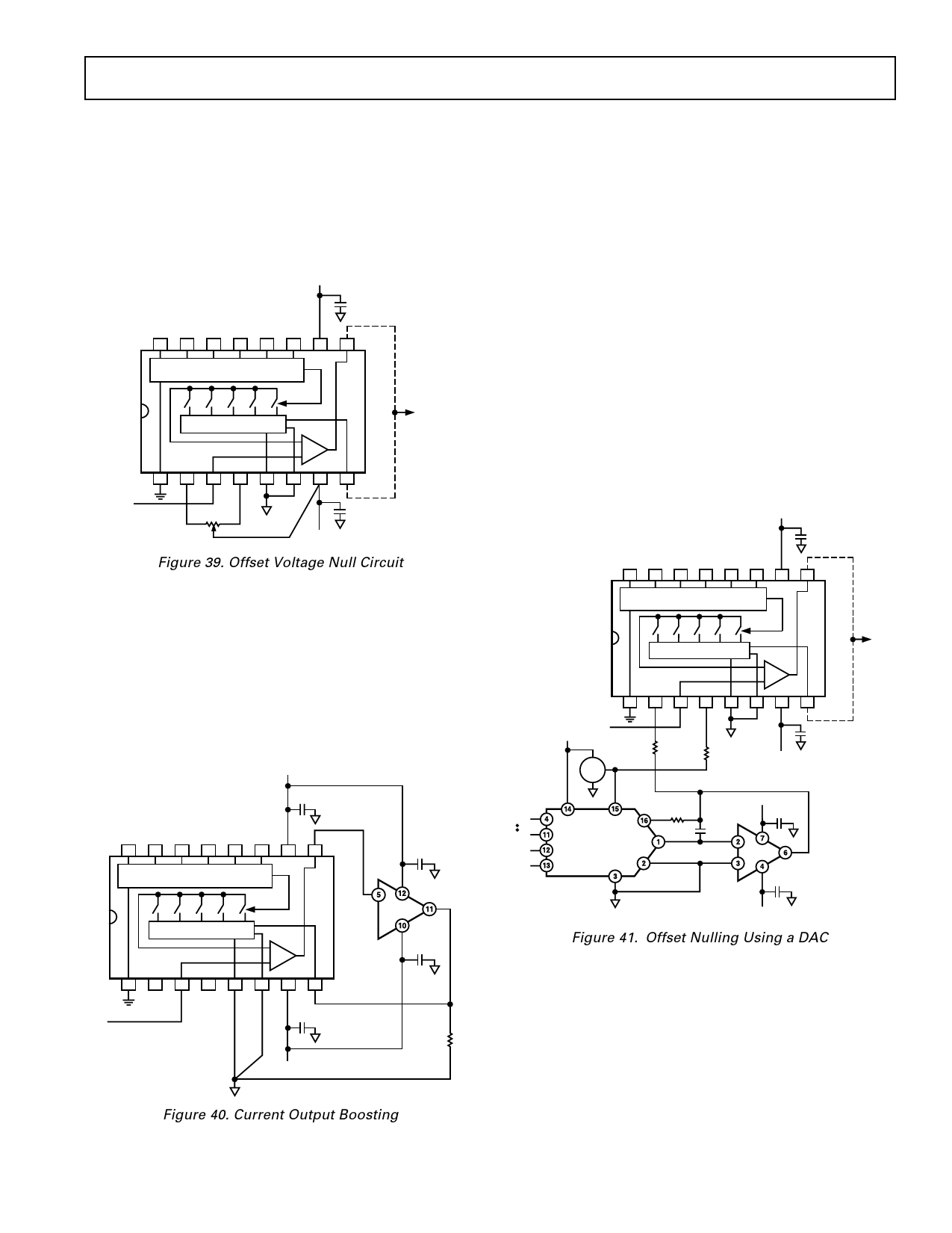
OFFSET NULLING WITH A D/A CONVERTER
Figure 41 shows the AD526 with offset nulling accomplished
with an 8-bit D/A converter (AD7524) circuit instead of the
potentiometer shown in Figure 39. The calibration procedure is
the same as before except that instead of adjusting the potenti-
ometer, the D/A converter corrects for the offset error. This
calibration circuit has a number of benefits in addition to elimi-
nating the trimpot. The most significant benefit is that calibra-
tion can be under the control of a microprocessor and therefore
can be implemented as part of an autocalibration scheme. Sec-
ondly, dip switches or RAM can be used to hold the 8-bit word
after its value has been determined. In Figure 42 the offset null
sensitivity, at a gain of 16, is 80 µV per LSB of adjustment,
which guarantees dc accuracy to the 16-bit performance level.
MSB
LSB
CS
WR
+VS
0.1F
16 15 14 13 12 11 10
A1 A0 CS CLK A2 B
LOGIC AND LATCHES
OUT
9 FORCE
16 8 4 2 1
GAIN NETWORK
–
AD526
+
VOUT
1
+VS VIN
AD581 OR
AD587
+10V
VREF
AD7524
2 3 4 5 6 7 8 OUT
SENSE
3.3M⍀
7.5M⍀
0.1F
–VS
1k⍀
ALL BYPASS CAPACITORS ARE 0.1F
+VS
0.01F
OUT 1
OUT 2
10F
–
AD548
+
0.01F
GND
–VS
Figure 41. Offset Nulling Using a DAC
Figure 40. Current Output Boosting
REV. D
–11–
Share Link: 