AD7570 데이터 시트보기 (PDF) - Analog Devices
부품명
상세내역
제조사
AD7570 Datasheet PDF : 12 Pages
| |||
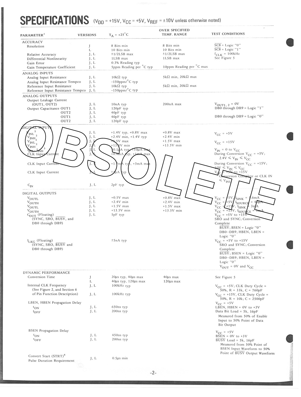
SPECIFICATIONS(VOO0=+15V, VCC 0=+5V, VREF0=:!:lOV unless otherwise noted)
PARAMETERI
VERSIONS
TA = +25°C
OVER SPECIFIED
TEMP. RANGE
' '--
TEST CONDITIONS
-
ACCURACY
Resolution
Relative Accuracy
Differential Nonlinearity
Gain Error
Gain Temperature Coefficient
ANALOG INPUTS
Analog Input Resistance
Analog Input Resistance Tempco
Reference Input Resistance
J
8 Bits min
L
10 Bits min
J, L
:!:1/2LSB max
1.L
ILSB max
J, L
0.3% Reading typ
J, L---------------- 5ppm Reading per 0 C typ
J, L
10kQ typ
1.L
-150ppm/C typ
J, L
10kQ typ
8 Bits min
10 Bits min
:!:1/2LSB max
ILSB max
----1-0--p-p.-m.----R--e-a-d--i.n--g---p--er 0 C max
5kQ Olin, 20kQ max
5kQ min, 20kQ max
SC8 = Logic "0"
SC8 = Logic "I"
fCLK = 100kHz
See Figure 5
Reference Input Resistance Tempco J, L
-I 5.9"p_n1/C- ty I' ---------------
ANALOG OUTPUTS
Output Leakage Current
(OUT!, OUT2)
J, L
lUnA typ
200nA max
Voun, 2 = OV
Output Capacitance OUTI
J, L
120pF typ
DBOthrough DB9 = Logic "I"
OUT2
1.L
40pF typ
OBSOLETE DIGITAL INPUTS
VINL 2
VINH2
VINL2
VINH2
IINL' IINH 3
CLK Input Current
OUT!
OUT2
CLK Input Current
CLK Input Current
Cm
u
DIGITAL OUTPUTS
VOUTL
YOUTH
VOUTL
1.L
J, L
1.L
J, L
J, L
J, L
J, L
J, L
J, L
1.L
J, L
---.
J, L
1.L
1.L
40pF typ
120pF typ
----------.-
+1.4V typ, +0.8V max
+2.4V min, + 1.4V typ
+1.5V max
+13-5V min
:!:O_IIlA typ, :!:IOIlA max
+0.4011\ typ, +lmA max
+1.7m1\ typ, +3mA max
:!:IIlA typ
2pF typ
+0.5V max
+2.4V min
+1.5V max
+0_8V max
+2.4V Olin
+ 1.5V max
+ 13.5V min
+0_8V max
+2.4V min
+1.5V max
DBO through DB9 = Logic "0"
Vcc = +5V
Vcc = +15V
VIN = 0 to VCC
During Conversion Vcc = +5V;
2_4V « VIN « Vcc
During Conversion VCC = +15V;
10V « VIN « VCC
Vcc = +5V to +15V
Conversion Complete or CLK IN
« VINL
Vcc = +5V, ISINK = 1.6mA
VCC = +5V, IsOURCE = 40llA
VCC = +15V, ISINK = 3mA
YOUTH
J, L
+13.5V min
+13.5V min
VCC = +15V, ISOURCE = ImA
CoUT (Floating) -
J, L
5pF typ
VCC = +5V to +15V
(SYNC, SRO, BUSY, and
SRO and SYNC; Conversion
DBO thro~gh DB9)
Complete
BUSY; BSEN = Logic "0"
DBO-DB9; HBEN, LBEN =
Logic "0"
ILKG (Floating)
(SYNC, SRO, BUSY and
:!:5nA typ
VCC = +5V to +15V
SRO and SYNC; Conversion
DBO through DB9)
Complete
BUSY; BSEN = Logic "0"
DBO-DB9; HBEN, LBEN =
Logic "0"
VOUT = OV and VCC
DYNAMIC PERFORMANCE
Conversion Time
Internal CLK Frequency
(See Figure 2, and Section 6
of Pin Function Description)
LBEN, HBEN Propagation Delay
tON
IoFF
J
L
J, L
1.L
J, L
1.L
20lls typ, 40lls max
40lls typ, 120lls max
100kHz typ
100kHz typ
650ns typ
200ns typ
40lls max
120llS max
See Figure 5
Vcc = +5V; CLK Duty Cycle =
50%, R = 33k, C = 760pF
VCC = +15V, CLK Duty Cycle =
= 50%, R lOk; C = 2500pF
Vcc = +5V
LBEN, HBEN = OV to +3V
Data Bit Load = 5k, 16pF
Measured from 50% of Enable
Input to 50% Point of Data
Bit Output
BSEN Propagation Delay
tON
tOFF
Convert Start (STRT)4
Pulse Duration Requirement
J, L
450ns typ
1.L
200ns ryp
J, L
0.51ls Olin
Vcc = +5V
BSEN = OV to +3V
BUSY Load = 5k, 16pF
Measured from 50% Point of
BSEN Input Waveform to 50%
Point of BUSY Output Waveform
-2-
--
8
I
I
t
,'
-~
"~.--
W
i-
Share Link: 