AD8517 데이터 시트보기 (PDF) - Analog Devices
부품명
상세내역
제조사
AD8517 Datasheet PDF : 12 Pages
| |||
AD8517/AD8527
DRIVING CAPACITIVE LOAD
Gain vs. Capacitive Load
Most amplifiers have difficulty driving capacitance due to degradation
of phase caused by additional phase lag from the capacitive load.
Higher capacitance at the output can increase the amount of over-
shoot and ringing in the amplifier’s step response and could even
affect the stability of the device. The value of capacitance load an
amplifier can drive before oscillation varies with gain, supply volt-
age, input signal, temperature, and frequency, among others. Unity
gain is the most challenging configuration for driving capacitance
load. However, the AD8517 offers good capacitance driving ability.
Table II shows the AD8517’s ability to capacitance load at differ-
ent gains before instability occurs. This table is good for all VSY.
Table II. Gain and Capacitance Load
Gain
1
2
2.5
3
Max Capacitance
400 pF
1.5 nF
8 nF
Unconditionally Stable
In-the-Loop Compensation Technique for Driving
Capacitive Loads
When driving capacitive loads in unity configuration, the in-the-
loop compensation technique is recommended to avoid oscillation
as is illustrated in Figure 22.
RF
RG
VIN
CF
AD8517
RX
VOUT
CL
RX =
RO RG
RF
WHERE RO = OPEN-LOOP OUTPUT RESISTANCE
ͩ ͪ ͩ ͪ 1
CF = 1 + ACL
RF + RG
RF
CLRO
Figure 22. In-the-Loop Compensation Technique for
Driving Capacitive Loads
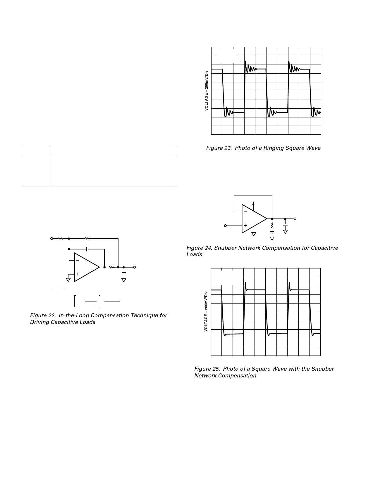
Snubber Network Compensation for Driving Capacitive Loads
As load capacitance increases, the overshoot and settling time
will increase and the unity gain bandwidth of the device will
decrease. Figure 23 shows an example of the AD8517 config-
ured for unity gain and driving a 10 kΩ resistor and a 680 pF
capacitor placed in parallel, with a square wave input set to a
frequency of 250 kHz and unity gain.
F = 250kHz
AV = +1
C = 680pF
TIME – 1s/Div
Figure 23. Photo of a Ringing Square Wave
By connecting a series R–C from the output of the device to
ground, known as the “snubber” network, this ringing and over-
shoot can be significantly reduced. Figure 24 shows the network
setup, and Figure 25 shows the improvement of the output
response with the “snubber” network added.
5V
AD8517
VOUT
VIN
RX
CL
CX
Figure 24. Snubber Network Compensation for Capacitive
Loads
F = 250kHz
AV = +1
C = 680pF
TIME – 1s/Div
Figure 25. Photo of a Square Wave with the Snubber
Network Compensation
The network operates in parallel with the load capacitor, CL,
and provides compensation for the added phase lag. The actual
values of the network resistor and capacitor have to be empiri-
cally determined. Table III shows some values of snubber network
for large capacitance load.
–10–
REV. B
Share Link: 