AD8517 데이터 시트보기 (PDF) - Analog Devices
부품명
상세내역
제조사
AD8517 Datasheet PDF : 12 Pages
| |||
AD8517/AD8527
D1
؊IN
D2
R7
R8
ESD
I1
D3
ESD
R3
R4
R1 Q3 Q1 Q2 Q4 R2
D7
R5
R6
D8
D4
ESD
ESD
R9
I2
R10
VCC
Q5
؉IN
C1
Q8
Q6
I3
Q11
Q10
Q9
I4
I7
Q7
Q14
Q13
R14
I8
Q19
Q20
C4
C3
C2
Q18
R11
Q17
Q15
D16
I5
I6 R12
R13
VEE
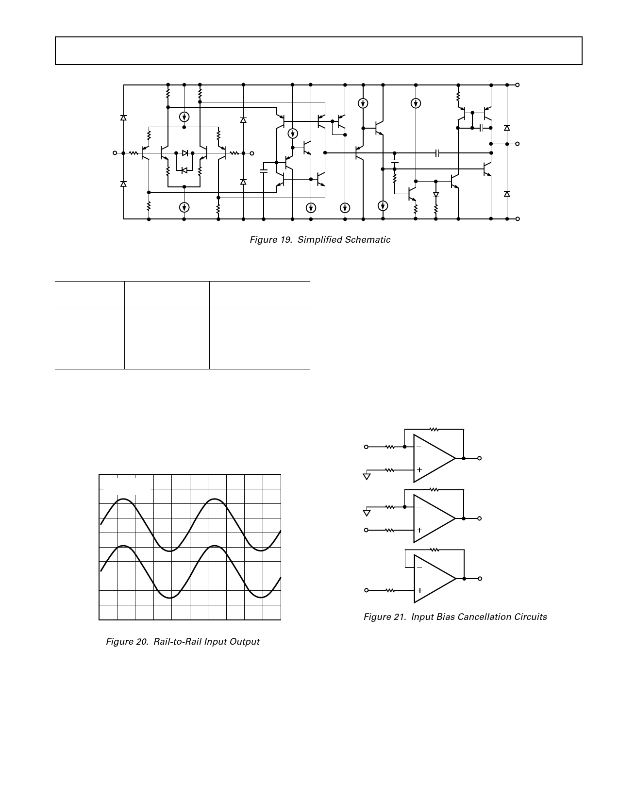
Figure 19. Simplified Schematic
VCC
D9
VOUT
D6
VEE
Table I. Typical Battery Life Voltage Range
Battery
Lead-Acid
Lithium
NiMH
NiCd
Carbon-Zinc
Nominal
Voltage (V)
2
2.6-3.6
1.2
1.2
1.5
End of Voltage
Discharge (V)
1.8
1.7-2.4
1
1
1.1
RAIL-TO-RAIL INPUT AND OUTPUT
The AD8517 features an extraordinary rail-to-rail input and
output with supply voltages as low as 1.8 V. With the amplifier’s
supply range set to 1.8 V, the input can be set to 1.8 V p-p,
allowing the output to swing to both rails without clipping. Figure
20 shows a scope picture of both input and output taken at unity
gain, with a frequency of 1 kHz, at VS = 1.8 V and VIN = 1.8 V p-p.
VS = ؎0.9V
VIN = 1.8 V p-p
VIN
INPUT BIAS CONSIDERATION
The input bias current (IB) is a nonideal, real-life parameter that
affects all op amps. IB can generate a somewhat significant offset
voltage. This offset voltage is created by IB when flowing through
the negative feedback resistor RF. If IB is 500 nA (worst case),
and RF is 100 kΩ, the corresponding generated offset voltage is
50 mV (VOS = IB ϫ RF).
Obviously the lower RF the lower the generated voltage offset.
Using a compensation resistor, RB, as shown in Figure 21, can
significantly minimize this effect. With the input bias current mini-
mized, we still need to be aware of the input offset current (IOS)
which will generate a slight offset error. Figure 21 shows three
different configurations to minimize IB-induced offset errors.
RF
RI
VI
RB = RIԽԽRF
AD8517
VOUT
INVERTING CONFIGURATION
RF
RI
RB = RIԽԽRF AD8517
VOUT
VI
NONINVERTING CONFIGURATION
RF = RS
VOUT
TIME – 200s/Div
Figure 20. Rail-to-Rail Input Output
The rail-to-rail feature of the AD8517 can be observed over the
supply voltage range, 1.8 V to 5 V. Traces are shown offset for
clarity.
RS
AD8517
VOUT
VI
UNITY GAIN BUFFER
Figure 21. Input Bias Cancellation Circuits
REV. B
–9–
Share Link: 