ADP121-ACBZ155R7 데이터 시트보기 (PDF) - Analog Devices
부품명
상세내역
제조사
ADP121-ACBZ155R7 Datasheet PDF : 20 Pages
| |||
THEORY OF OPERATION
The ADP121 is a low quiescent current, low dropout linear
regulators that operate from 2.3 V to 5.5 V and provide up
to 150 mA of output current. Drawing a low 30 μA quiescent
current (typical) at full load makes the ADP121 ideal for battery-
operated portable equipment. Shutdown current consumption
is typically 100 nA.
Optimized for use with small 1 μF ceramic capacitors,
the ADP121 provides excellent transient performance.
VIN
VOUT
R1
GND
SHORT CIRCUIT,
UVLO, AND
THERMAL
PROTECT
EN
SHUTDOWN
0.8V REFERENCE
R2
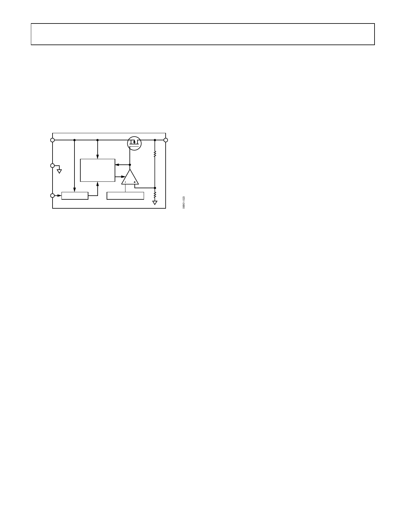
Figure 27. Internal Block Diagram
ADP121
Internally, the ADP121 consists of a reference, an error amplifier,
a feedback voltage divider, and a PMOS pass transistor. Output
current is delivered via the PMOS pass device, which is con-
trolled by the error amplifier. The error amplifier compares the
reference voltage with the feedback voltage from the output and
amplifies the difference. If the feedback voltage is lower than
the reference voltage, the gate of the PMOS device is pulled
lower, allowing more current to flow and increasing the output
voltage. If the feedback voltage is higher than the reference
voltage, the gate of the PMOS device is pulled higher, allowing
less current to flow and decreasing the output voltage.
The ADP121 is available in 16 output voltage options ranging
from 1.2 V to 3.3 V. The ADP121 uses the EN pin to enable and
disable the VOUT pin under normal operating conditions.
When EN is high, VOUT turns on; when EN is low, VOUT
turns off. For automatic startup, EN can be tied to VIN.
Rev. 0 | Page 11 of 20
Share Link: 