BD6761FS 데이터 시트보기 (PDF) - ROHM Semiconductor
부품명
상세내역
제조사
BD6761FS Datasheet PDF : 23 Pages
| |||
BD6761FS,BD6762FV
Technical Note
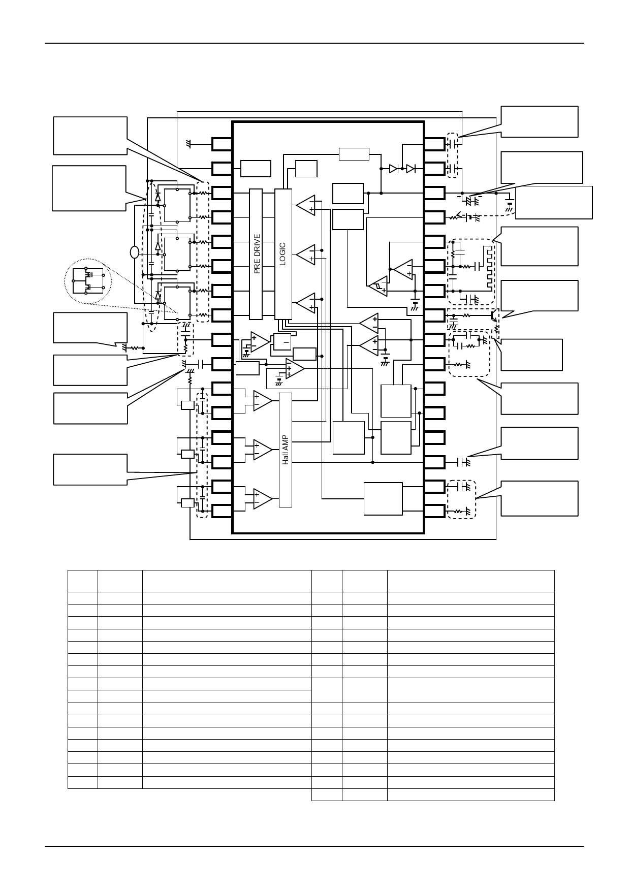
●Block Diagram, Application Circuit Diagram, and Pin Function
1)BD6761FS
⑮
Output FET gate
voltage stabilization
resistor
See P.19/22.
②③
Capacitor, diode for the
protection between the
output FET drain and
source
See P. 18/22.
0.1µF
M
0.1µF
①
MOS FET
⑧
0.1µF
Resistor for setting
the current limit
See P. 18/22.
0.12Ω
⑩
RNF
CL voltage smoothing
low pass filter
See P. 18/22.
⑯
Capacitor for setting
the peak hold
See P. 19/22.
⑨
Capacitor for Hall
noise elimination
See P. 18/22.
1pin
GND
MOS
FET
CP1
BOOSTER
UHG
ULG
TSD
MOS
FET
VHG
VLG
MOS
FET
WHG
WLG
470pF
CL
1k
0.033µF
(0.01µF ~ 0.1µF)
PH
200Ω
R2 (200Ω
~ 1kΩ)
HU+
0.01µF
HU
HU-
CURRENT
LIMIT
SQ
VCL2
RQ
EDGE
DETECT
PEAK
HOLD
VCL1
CURRENT
SENSE AMP
HV+
0.01µF
HV
HV-
HW+
0.01µF
HW
HW-
16pin
UVLO
REGURATOR
10.5V
REGURATOR
10.5V
OUTPUTOFF
COMP
TORQUE
AMP
SLEW
RATE
DETECT
CHARGE
PUMP
SHORT
BRAKE
TRAIANGLE
WAVE
GENERATOR
④
Capacitor for setting
VG current capacity
32pin
See P. 18/22.
CP2
0.01µF
⑬
(0.01µF ~ 0.1µF)
0.1µF
VG
Capacitor for VCC pin
noise elimination
See P. 19/22.
VCC
10µF
FGSOUT
10kΩ
(1kΩ ~ 100kΩ)
470pF
FGOUT
R2
82kΩ
C2
1500pF
FGIN-
FGIN+
R1
820Ω C1
470pF 0.47µF
0.22µF
VREG
CPOUT
RCP
1kΩ
0.1µF
(0.01µF~0.1µF)
C3
0.022µ
C4
R3
0.33µF 100kΩ
100kΩ
ACC
DEC
F/R
CNF
0.1µF
FGSOUT pull-up
resistor
See P. 20/22.
⑪
Resistor for setting FG
amplifier gain and the
capacitor for the filter
See P. 18/22.
⑦
Capacitor for preventing
VREG oscillation
See P. 18/22.
R1 200Ω(200Ω ~ 1kΩ)
⑥
For setting Hall
input level
See P. 18/22.
⑭
Capacitor, resistor for
setting the charge pump
See P. 19/22.
⑫
Capacitor for setting the
phase compensation
See P. 19/22.
CFE
1000pF (500pF ~ 2000pF)
RFE
17pin
50kΩ
(50kΩ ~ 100kΩ)
⑤
External constant for
setting PWM frequency
See P. 18/22.
Fig.9 BD6761FS Block Diagram
BD6761FS pin Function
No.
Pin
name
Function
No.
Pin
name
Function
1
GND GND pin
17 RFE CFE current control pin
2
CP1 CP1 pin
18 CFE PWM frequency control pin
3
UHG U-phase high-side FET gate pin
19 CNF Phase compensation pin
4
ULG U-phase low-side FET gate pin
20
F/R Forward/reverse rotation switching pin
5
VHG V-phase high-side FET gate pin
21 DEC Deceleration signal input pin
6
VLG V-phase low-side FET gate pin
22 ACC Acceleration signal input pin
7 WHG W-phase high-side FET gate pin
23 RCP CPOUT current control pin
8
WLG W-phase low-side FET gate pin
9
CL Motor current detection pin
24
CPOUT
Charge pump output /
Torque control signal input pin
10
PH Peak hold pin
25 VREG VREG pin
11 HU+ Hall signal input pin
26 FGIN+ FG input + pin
12
HU- Hall signal input pin
27 FGIN- FG input - pin
13 HV+ Hall signal input pin
28 FGOUT FG output pin
14
HV- Hall signal input pin
29 FGSOUT FGS output pin
15 HW+ Hall signal input pin
30 VCC VCC pin
16 HW- Hall signal input pin
31
VG Boost pin
32 CP2 CP2 pin
www.rohm.com
© 2010 ROHM Co., Ltd. All rights reserved.
6/22
2010.06 - Rev.A
Share Link: 