CDP1802AC/3 데이터 시트보기 (PDF) - Intersil
부품명
상세내역
제조사
CDP1802AC/3 Datasheet PDF : 27 Pages
| |||
CDP1802AC/3
by connecting an RC network directly to the CLEAR pin, since it
has a Schmitt triggered input; see Figure 20.
VCC
RS
CDP1802
CLEAR
3
C
THE RC TIME CONSTANT
SHOULD BE GREATER THAN
THE OSCILLATOR START-UP
TIME (TYPICALLY 20ms)
FIGURE 20. RESET DIAGRAM
PAUSE
Stops the internal CPU timing generator on the first negative
high-to-low transition of the input clock. The oscillator
continues to operate, but subsequent clock transitions are
ignored.
RUN
May be initiated from the Pause or Reset mode functions. If
initiated from Pause, the CPU resumes operation on the first
negative high-to-low transition of the input clock. When
initiated from the Reset operation, the first machine cycle
following Reset is always the initialization cycle. The
initialization cycle is then followed by a DMA (S2) cycle or
fetch (S0) from location 0000 in memory.
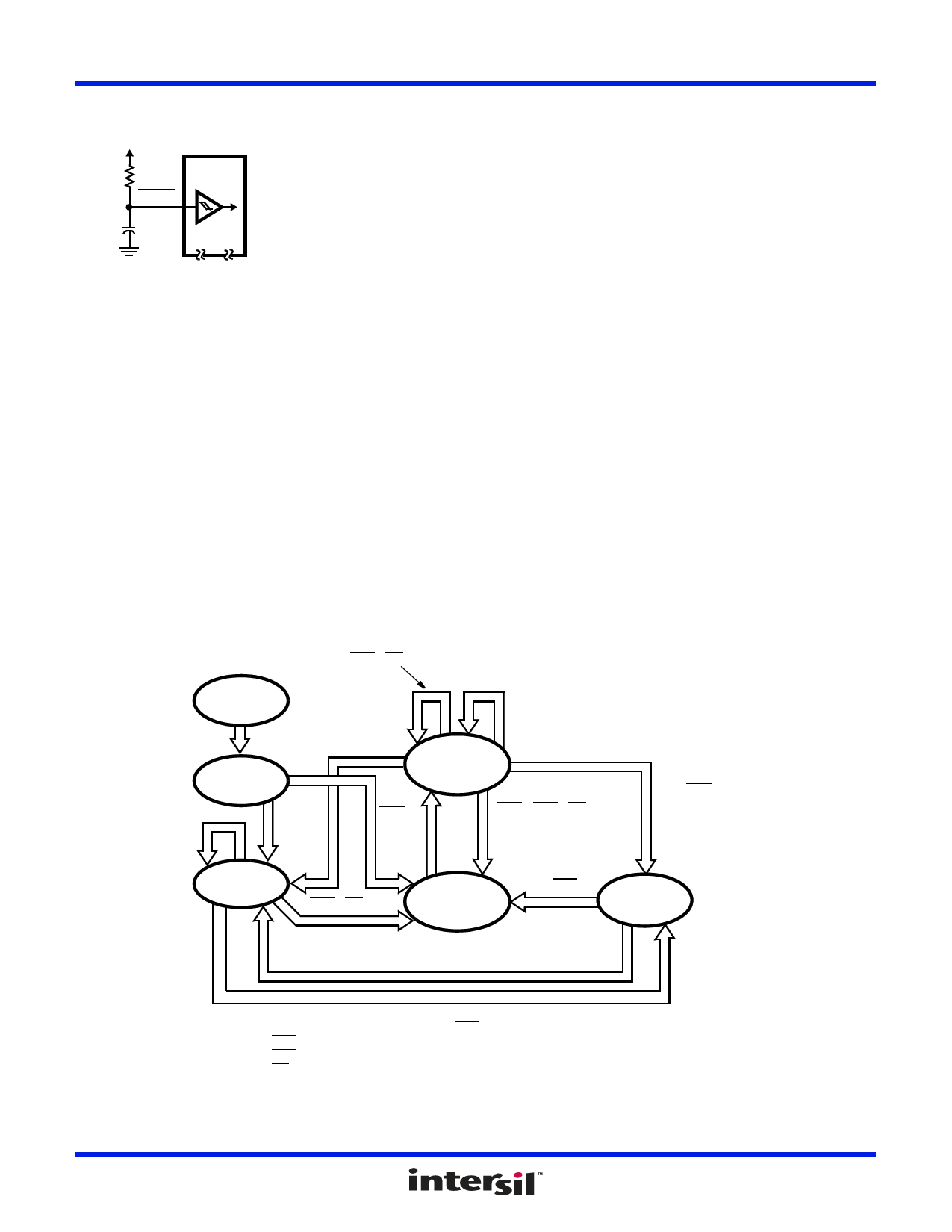
RUN-MODE STATE TRANSITIONS
The CPU state transitions when in the RUN and RESET
modes are shown in Figure 21. Each machine cycle requires
the same period of time, 8-clock pulses, except the
initialization cycle, which requires 9-clock pulses. The
execution of an instruction requires either two or three
machine cycles, S0 followed by a single S1 cycle or two S1
cycles. S2 is the response to a DMA request and S3 is the
interrupt response. Table 5 shows the conditions on Data
Bus and Memory Address lines during all machine states.
INSTRUCTION SET
The CPU instruction summary is given in Table 4.
Hexadecimal notation is used to refer to the 4-bit binary
codes.
In all registers bits are numbered from the least significant bit
(LSB) to the most significant bit (MSB) starting with 0.
R(W): Register designated by W, where:
W = N or X, or P
R(W).0: Lower order byte of R(W)
R(W).1: Higher order byte of R(W)
OPERATION NOTATION
M(R(N)) D; R(N) + 1 R(N)
This notation means: The memory byte pointed to by R(N) is
loaded into D, and R(N) is incremented by 1.
S1 RESET
IDLE DMA INT
.
FORCE S1
(LONG BRANCH,
LONG SKIP, NOP, ETC.)
S1 INIT
DMA
DMA
DMA
S1 EXECUTE
DMA
DMA IDLE INT
INT DMA
S2 DMA
DMA INT
S0 FETCH
DMA
DMA
S3 INT
PRIORITY: FORCE S0, S1
DMA IN
DMA OUT
INT
INT DMA
FIGURE 21. STATE TRANSITION DIAGRAM
FN1441 Rev 3.00
October 17, 2008
Page 18 of 27
Share Link: 