M56759FP 데이터 시트보기 (PDF) - MITSUBISHI ELECTRIC
부품명
상세내역
제조사
M56759FP Datasheet PDF : 11 Pages
| |||
MITSUBISHI <CONTROL / DRIVER IC>
M56759FP/AFP
4-CHANNEL ACTUATOR DRIVER
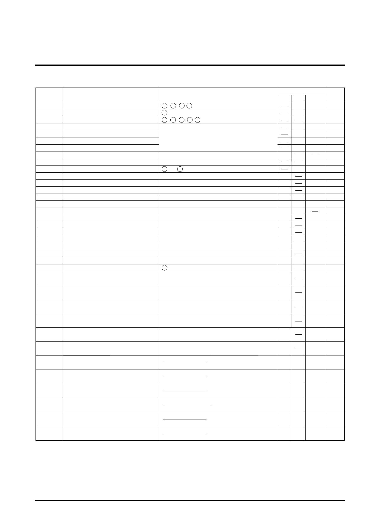
ELECTRICAL CHARACTERISTICS
(Ta=25˚C, VCC1=Vm1=Vm2=Vm3=5V, VCC2=12V, no-load current
unless otherwise noted)
Symbol
Parameter
Conditions
ICC1
Supply current-1
1 , 26 , 15, 6 pins supply current (Vref=Vctl=2.5V)
ICC2
Supply current-2
23 pins[VCC1] supply current (Vref=Vctl=2.5V)
ICC3
Sleep Mode Supply current-3
1 , 23 , 26 , 15 , 6 pins supply current (MUTE1,2=H)
VsatCH1 Ch1 Saturation voltage
VsatCH2 Ch2 Saturation voltage
Top and Bottom saturation voltage.
VsatCH3 Ch3 Saturation voltage
Load current 500mA. At bootstrap.
VsatCH4 Ch4 Saturation voltage
Vmute-on Mute-on voltage
Mute-on
Vmute-off Mute-off voltage
Mute-off
Imute Mute terminals input current
41 and 42 pin input current at 5V input voltage.
VinOP OP1 and OP2 amplifier Input voltage range
VoutOP OP1 and OP2 amplifier output voltage range Io=±2.0mA
VofOP OP1 and OP2 amplifier input offset voltage Vin=2.5V (at buffer)
IinOP OP1 and OP2 amplifier input current
inverted input = non-inverted input = 2.5V
IofOP OP1 and OP2 amplifier input current offset inverted input = non-inverted input = 2.5V
GBOP OP1 and OP2 amplifier GB
VinE
E1,E2 and E3 amplifier Input voltage range
VoutE E1,E2 and E3 amplifier output voltage range No load
VofE
E1,E2 and E3 amplifier input offset voltage Vin=2.5V (at buffer)
IinE
E1,E2 and E3 amplifier input current
inverted input = non-inverted input = 2.5V
IofE
E1,E2 and E3 amplifier input current offset inverted input = non-inverted input = 2.5V
VoutS S1 and S2 amplifier output voltage range No load
VinVREF VREF buffer amplifier Input voltage range
VofVREF VREF buffer amplifier offset voltage
2 pin input voltage = 2.5V
Limits
Min. Typ. Max.
24 36
9.5 15
500
0.8 1.20
0.8 1.20
0.5 0.9
0.6 1.0
2.0
0.8
170 250
0.5
VCC2-1.0
0.5
VCC1-0.5
-10
+10
-1.0 -0.15 0
-100 0 +100
2.3 4
0.5
VCC2-2.0
1.0
VCC1-0.5
-10
+10
-1.0 -0.15 0
-100 0 +100
1.0
VCC1-0.5
1.5 2.5 VCC1-1.2
-10
+10
Unit
mA
mA
µA
V
V
V
V
V
V
µA
V
V
mV
µA
nA
MHz
V
V
mV
µA
nA
V
V
mV
VofCH1 Ch1 output offset voltage
when the OUT1 voltage is adjusted at the same
VREFO voltage, at VREF=2.5V
-26
+26 mV
VofCH2 Ch2 output offset voltage
when the OUT2 voltage is adjusted at the same
VREFO voltage, at VREF=2.5V
-26
+26 mV
VofCH3 Ch3 output offset voltage
when the OUT3 voltage is adjusted at the same
VREFO voltage, at VREF=2.5V
-26
+26 mV
VofCH4 Ch4 output offset voltage
when the IN4- voltage is adjusted at the same
VREFO voltage, at VREF=2.5V
-26
+26 mV
VofS1 S1 output offset voltage
SOUT1-VREFO (at SI N1[-] = VM1[+] )
at VREF=2.5V
-20
+20 mV
VofS2 S2 output offset voltage
SOUT2-VREFO (at SI N2[-] = VM2[+] )
at VREF=2.5V
-20
+20 mV
GainCH1 Ch1 power amplifier voltage gain
{VM1(+)–VM1(-)}
(OUT1–VREFO)
at VREF=2.5V
13.1 14 14.8 dB
GainCH2 Ch2 power amplifier voltage gain
{VM2(+)–VM2(-)}
(OUT2–VREFO)
at VREF=2.5V
13.1 14 14.8 dB
GainCH3 Ch3 power amplifier voltage gain
{VM3(+)–VM3(-)}
(OUT3–VREFO)
at VREF=2.5V
19.1 20 20.8 dB
GainCH4 Ch4 power amplifier voltage gain
-1 · {VM4(+)–VM4(-)}
(I N4A[-]–VREFO)
at VREF=2.5V
3.17 4.08 4.91 dB
GainS1 S1 amplifier voltage gain
GainS2 S2 amplifier voltage gain
{SOUT1 - VREFO}
(VM1[+] - SI N1[-] )
{SOUT2 - VREFO}
(VM2[+] - SI N2[-] )
at VREF=2.5V
at VREF=2.5V
5.11 6.02 6.85 dB
5.11 6.02 6.85 dB
Share Link: 