ICL7112 데이터 시트보기 (PDF) - Intersil
부품명
상세내역
제조사
ICL7112 Datasheet PDF : 14 Pages
| |||
ICL7112
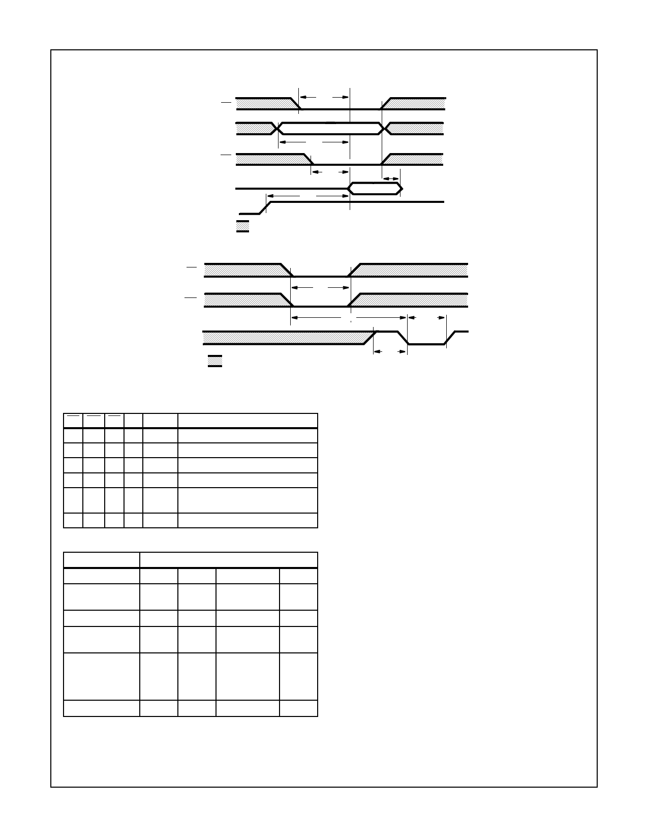
Timing Diagrams
CS
A0
RD
D0 - D13
EOC
tCD
VALID
tAD
tRD
tED
tRX
VALID
= DON’T CARE
FIGURE 1. READ CYCLE TIMING
CS
WR
EOC
tWR
tWE
tCONV
tEO
= DON’T CARE
FIGURE 2. WRITE CYCLE TIMING
TABLE 2: I/O CONTROL
CS WR RD A0
0 0 xx
1 x xx
0 x 00
0 x 01
0 x 0x
x x 1x
BUS
x
x
0
0
1
x
FUNCTION
Initiates a conversion.
Disables all chip commands.
Low byte is enabled.
High byte is enabled.
Low and High bytes enabled togeth-
er.
Disables outputs (high-impedance).
TABLE 3: TRANSFER FUNCTION
INPUT VOLTAGE
VREF = -10.0V
0
+0.00244
+0.30029
+4.99756
+5.00000
+9.99512
+9.99756
+10.00000
+10.00244
+10.29000
EXPECTED OUTPUT CODE
OVR MSB
LSB
0
0
0000000000
0
0
0
0000000000
1
0
0
0000111101
1
0
0
1111111111
1
0
1
0000000000
0
0
1
1111111111
0
0
1
1111111111
1
1
0
0000000000
0
1
0
0000000000
1
1
0
0000111101
1
Detailed Description
The ICL7112 is basically a successive approximation A/D
converter with an internal structure much more complex than
a standard SAR-type converter. The Functional Block Dia-
gram shows the functional diagram of the ICL7112 12-bit
A/D converter. The additional circuitry incorporated into the
ICL7112 is used to perform error correction and to maintain
the operating speed in the 40µs range.
The internal DAC of the ICL7112 is designed around a radix
of 1.85, rather than the traditional 2.00. This radix gives each
bit of the DAC a weight of approximately 54% of the previous
bit. The result is a usable range that extends to 3% beyond
the full-scale input of the A/D. The actual value of each bit is
measured and stored in the on-chip PROM. The absolute
value of each bit weight then becomes relatively unimportant
because of the error correction action of the ICL7112.
The output of the high-speed auto-zeroed comparator is fed
to the data input of a successive approximation register
(SAR). This register is uniquely designed for the ICL7112 in
that it tests bit pairs instead of individual bits in the manner of
a standard SAR. At the beginning of the conversion cycle,
the SAR turns on the MSB (D11) and the MSB 4-bit (D7).
The sequence continues for each bit pair, BX and Bx-4, until
only the four LSBs remain. The sequence concludes by test-
ing the four LSBs individually.
The SAR output is fed to the DAC register and to the prepro-
grammed PROM where it acts as PROM address. PROM
data is fed to a full-adder/accumulator where the decoded
results from each successive phase of the conversion are
summed with the previous results. After 20 clock cycles, the
accumulator contains the final binary data which is latched
and sent to the three-state output buffers. The accuracy of
the A/D converter depends primarily upon the accuracy of
the data that has been programmed into the PROM during
6-6
Share Link: 