ICL7112 데이터 시트보기 (PDF) - Intersil
부품명
상세내역
제조사
ICL7112 Datasheet PDF : 14 Pages
| |||
ICL7112
the final test portion of the manufacturing process.
The error correcting algorithm built into the ICL7112 reduces
the initial accuracy requirements of the DAC. The overlap in
the testing of bit pairs reduces the accuracy requirements on
the comparator which has been optimized for speed. Since
the comparator is auto-zeroed, no external adjustment is
required to get ZERO code for ZERO input voltage.
Twenty clock cycles are required for the complete 12-bit con-
version. The auto-zero circuitry associated with the compar-
ator is employed during the last three clock cycles of the
conversion to cancel the effect of offset voltage. Also during
this time, the SAR and accumulator are reset in preparation
for the start of the next conversion.
The overflow output of the full-adder is also the OVer Range
(OVR) output of the ICL7112. Unlike standard SAR type A/D
converters, the ICL7112 has the capability of providing valid
usable data for inputs that exceed the fullscale range by as
much as 3%.
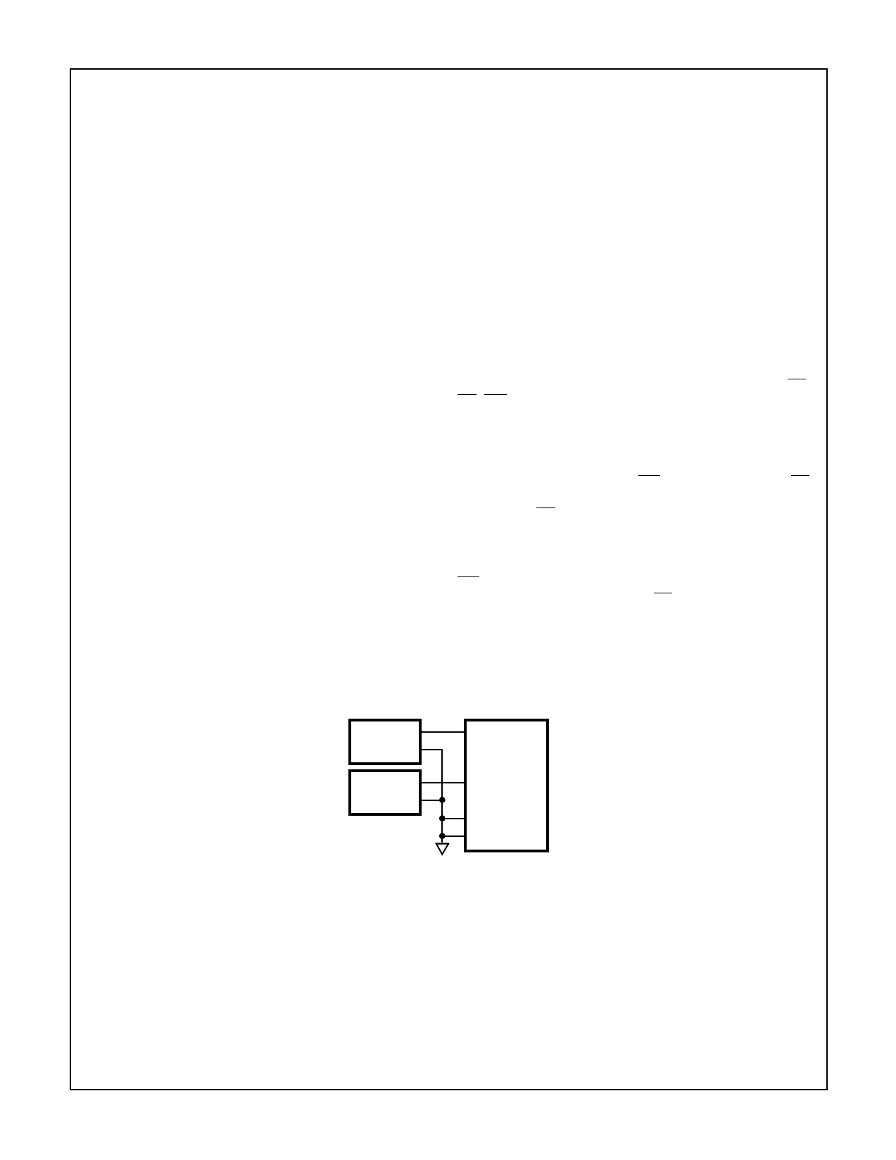
Optimizing System Performance
When using A/D converters with 12 or more bits of resolu-
tion, special attention must be paid to grounding and the
elimination of potential ground loops. A ground loop can be
formed by allowing the return current from the lCL7112’s
DAC to flow through traces that are common to other analog
circuitry. If care is not taken, this current can generate small
unwanted voltages that add to or detract from the reference
or input voltages of the A/D converter.
Figure 3 and Figure 4 show two different grounding tech-
niques. Although the difference between the two circuits may
not be readily apparent, the circuit of Figure 3 is very likely to
have significant ground loop errors which the circuit of Fig-
ure 4 avoids. In Figure 3, the supply currents for analog
ground, digital ground, and the reference voltage all flow
through a lead, common to the input. This will generate a DC
offset voltage due to the currents flowing in the resistance of
the common lead. This offset voltage will vary with the input
voltage and with the digital output. Even the auto-zero loop
of the ICL7112 cannot remove this error.
Figure 4 shows a much better arrangement. The ground and
reference currents do not flow through the input common
lead, eliminating any error voltages. Note that the supply
currents and any other analog system currents must also be
returned carefully to analog ground. The clamp diodes will
protect the ICL7112 against signals which could result from
separate analog and digital grounds. The absolute maximum
voltage rating between AGND and DGND is ±1.0V. The two
inverse-parallel diodes clamp this voltage to less than ±0.7V.
Input Warning
As with any CMOS integrated circuit, no input voltages
should be applied to the lCL7112 until the ±5V power sup-
plies have stabilized.
Interfacing To Digital Systems
The_ICL7112 provides three-state data output buffers, CS,
RD, WR, and bus select inputs (A0 and BUS) for interfacing
to a wide variety of microcomputers and digital systems. The
I/O Control Truth Table shows the functions of the digital
control lines. The BUS select and A0 lines are provided to
enable the output data onto either 8-bit or 16-bit data buses.
A conversion is initiated by a WR pulse (pin 33) when CS
(pin 3) is low. Data is enabled on the bus when the chip is
selected and RD (pin 4) is low.
Figure 5 illustrates a typical interface to an 8-bit microcom-
puter. The “Start and Wait” operation requires the fewest
external components and is initiated by a low level on the
WR input to the ICL7112 after the I/O or memory mapped
address decoder has brought the CS input low. After execut-
ing a delay or utility routine for a period of time greater than
the conversion time of the ICL7112, the processor issues
two consecutive bus addresses to read output data into two
bytes of memory. A low level on A0 enables the LSBs, and a
high level enables the MSBs.
VIN +
SOURCE -
VREF -
SOURCE +
VIN
ICL7112
VREF
AGND
DGND
FIGURE 3. IMPROPER GROUNDING TECHNIQUE WILL CAUSE GROUND LOOP ERRORS
6-7
Share Link: 