LT5521 데이터 시트보기 (PDF) - Linear Technology
부품명
상세내역
제조사
LT5521 Datasheet PDF : 16 Pages
| |||
LT5521
APPLICATIO S I FOR ATIO
0
–5
–10
C1 = 6.8pF
–15
–20
C1 = 2.7pF
–25
–30
–35
0
500 1000 1500 2000 2500 3000 3500 4000
FREQUENCY (MHz)
5521 F13
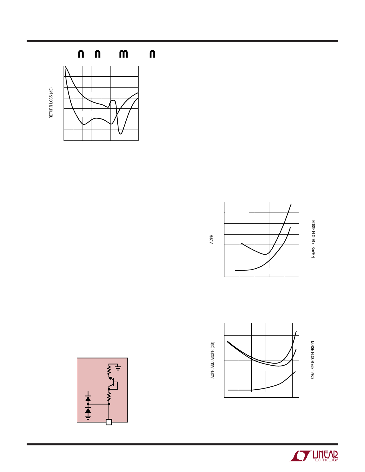
Figure 13. LO Port Return Loss
noise performance with slightly reduced current through
the mixer core. Accordingly, in a 5V application operating
within this LO frequency range, the recommended source
resistor value (R1 and R7) is increased to 121Ω.
Enable Interface
Figure 14 shows a simplified schematic of the EN pin
interface. The voltage necessary to turn on the LT5521 is
2.9V. To disable the chip, the enable voltage must be below
0.2V. If the EN pin is not connected, the chip is disabled.
It is not recommended, however, that any pins be left
floating for normal operation.
It is important that the voltage at the EN pin never exceed
VCC, the power supply voltage, by more than 0.2V. If this
should occur, the supply current could be sourced through
the EN pin ESD protection diodes, potentially damaging
the IC. The resistor R8 (Figure 1) in series with the EN pin
on the demo board is populated with a 10kΩ resistor to
protect the EN pin to avoid inadvertant damage to the IC.
For timing measurements, this resistor is replaced with a
LT5521
VCC
14
EN
5
5521 F14
Figure 14. Enable Input Circuit
0Ω resistor. If the shutdown function is not required, then
the EN pin should be wired directly to the VCC power supply
on the PCB.
Supply Decoupling
The power supply decoupling shown in the schematic of
Figure 1 is recommended to minimize spurious signal
coupling into the output through the power supply.
ACPR Performance
Because of its high linearity and low noise, the LT5521 offers
outstanding ACPR performance in a variety of applications.
For example, Figures 15 and 16 show ACPR and Alternate
Channel measurements for single channel and 4-channel
64 DPCH W-CDMA signals at 1.95GHz output frequency.
–30
TA = 25°C
–40
fRF = 1.95GHz
fIF = 70MHz
fLO = 1.88GHz
–50
–130
–135
–140
–60
–145
–70
–150
ACPR
–80
–155
–90
–100
–40
30MHz OFFSET NOISE
–30 –20 –10
0
OUTPUT CHANNEL POWER (dBm)
–160
–165
10
5521 F15
Figure 15. Single Channel W-CDMA ACPR
and 30MHz Offset Noise Performance
–50
–135
–55
–140
–60
–65
TA = 25°C
–70
fRF = 1.95GHz
fIF = 70MHz
fLO = 1.88GHz
–75
ACPR
AltCPR
–145
–150
–155
–160
30MHz OFFSET NOISE
–80
–165
–40 –35 –30 –25 –20 –15
OUTPUT CHANNEL POWER, EACH CHANNEL (dBm)
1635 G24
Figure 16. 4-Channel W-CDMA ACPR,
AltCPR and 30MHz Offset Noise Floor
5521f
Share Link: 