MAX9939 데이터 시트보기 (PDF) - Maxim Integrated
부품명
상세내역
제조사
MAX9939 Datasheet PDF : 15 Pages
| |||

SPI Programmable-Gain Amplifier
with Input VOS Trim and Output Op Amp
ABSOLUTE MAXIMUM RATINGS
VCC to GND ..............................................................-0.3V to +6V
INB, OUTA, OUTB, SCLK, DIN, CS............-0.3V to (VCC + 0.3V)
INA+, INA- to GND ..................................................-16V to +16V
Output Short-Circuit Current Duration........................Continuous
Continuous Input Current into Any Terminal.....................±20mA
Continuous Power Dissipation (TA = +70°C)
10-Pin µMAX (derate 5.6mW/°C above +70°C) ...........707mW
Operating Temperature Range .........................-40°C to +125°C
Junction Temperature ......................................................+150°C
Storage Temperature Range .............................-65°C to +150°C
Lead Temperature (soldering, 10s) .................................+300°C
Soldering Temperature (reflow) .......................................+260°C
Stresses beyond those listed under “Absolute Maximum Ratings” may cause permanent damage to the device. These are stress ratings only, and functional
operation of the device at these or any other conditions beyond those indicated in the operational sections of the specifications is not implied. Exposure to
absolute maximum rating conditions for extended periods may affect device reliability.
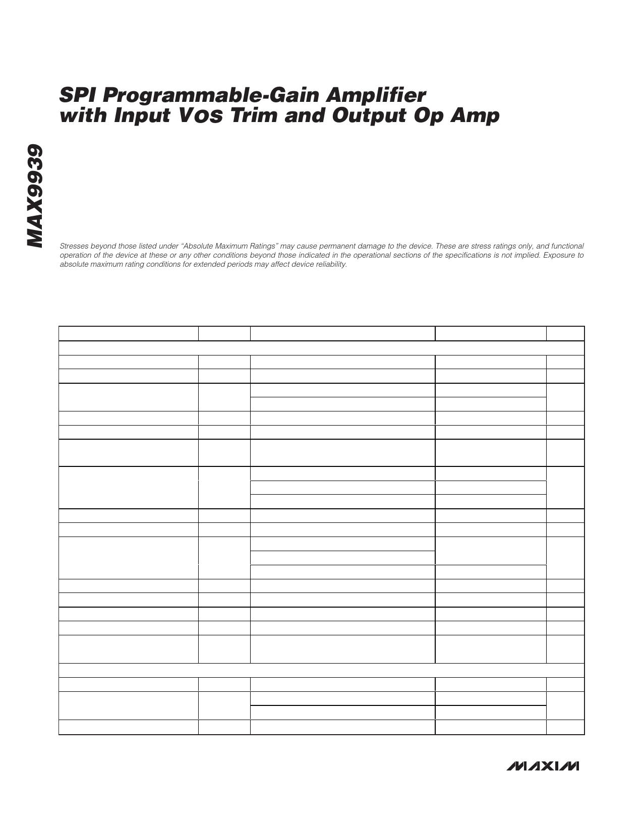
ELECTRICAL CHARACTERISTICS
(VCC = 5V, VGND = 0V, VINA+ = VINA-, Gain = 10V/V, ROUTA = ROUTB = 1kΩ to VCC/2, TA = TMIN to TMAX, unless otherwise noted.
Typical values are at TA = +25°C.) (Note 1)
PARAMETER
SYMBOL
CONDITIONS
MIN TYP MAX UNITS
PGA CHARACTERISTICS
Gain Error
Gain Temperature-Coefficient
Input Offset Voltage (Note 2)
Input Offset-Voltage Drift
Input Offset-Voltage Trim Range
GE
Tc-GE
VOS-A
TA = +25°C, 0.2V ≤ VOUTA ≤ VCC - 0.2V
With no VOS trim, TA = +25°C
With no VOS trim, TA = TMIN to TMAX
0.05 0.38
%
2.2
17 ppm/°C
1.5
9
mV
15
10
µV/C
±17
mV
Input Common-Mode Range
VCM Guaranteed by CMRR test (Note 3)
-VCC/2
VCC
- 2.2
V
Common-Mode Rejection Ratio
Output Short-Circuit current
Input-Voltage Noise Density
Gain-Bandwidth Product
CMRR
ISC
VN
GBW
-1V ≤ VCM ≤ VCC - 2.2V
-VCC/2 ≤ VCM ≤ VCC - 2.2V, TA = +25°C
-VCC/2 ≤ VCM ≤ VCC - 2.2V
f = 10kHz, gain = 157V/V
Gain = 0.2V/V
Gain = 1V/V
Gain = 157V/V
50
60
50
60
39
70
54
2.15
279
dB
mA
nV/√Hz
MHz
Slew Rate
Settling Time
Distortion
Max Capacitive Load
SR
tS
THD
CL(MAX)
To 1%, 2V output step
f = 1kHz, VOUTA = 2.5VP-P
9
V/µs
0.45
µs
89
dB
1
nF
Output Swing
VOH, VOL
OUTPUT AMPLIFIER CHARACTERISTICS
Voltage output high = VCC - VOUTA,
voltage output low = VOUTA - VGND
25
60
mV
Input Bias Current
Input Offset Voltage (Note 2)
Output Short-Circuit Current
Ib
VOS-B
ISC
(Note 4)
TA = +25°C
TA = TMIN to TMAX
1
pA
1.5
9
mV
15
70
mA
2 _______________________________________________________________________________________