MT46H16M16 데이터 시트보기 (PDF) - Micron Technology
부품명
상세내역
제조사
MT46H16M16 Datasheet PDF : 79 Pages
| |||
256Mb: x16, x32 Mobile DDR SDRAM
FBGA Part Marking Decoder
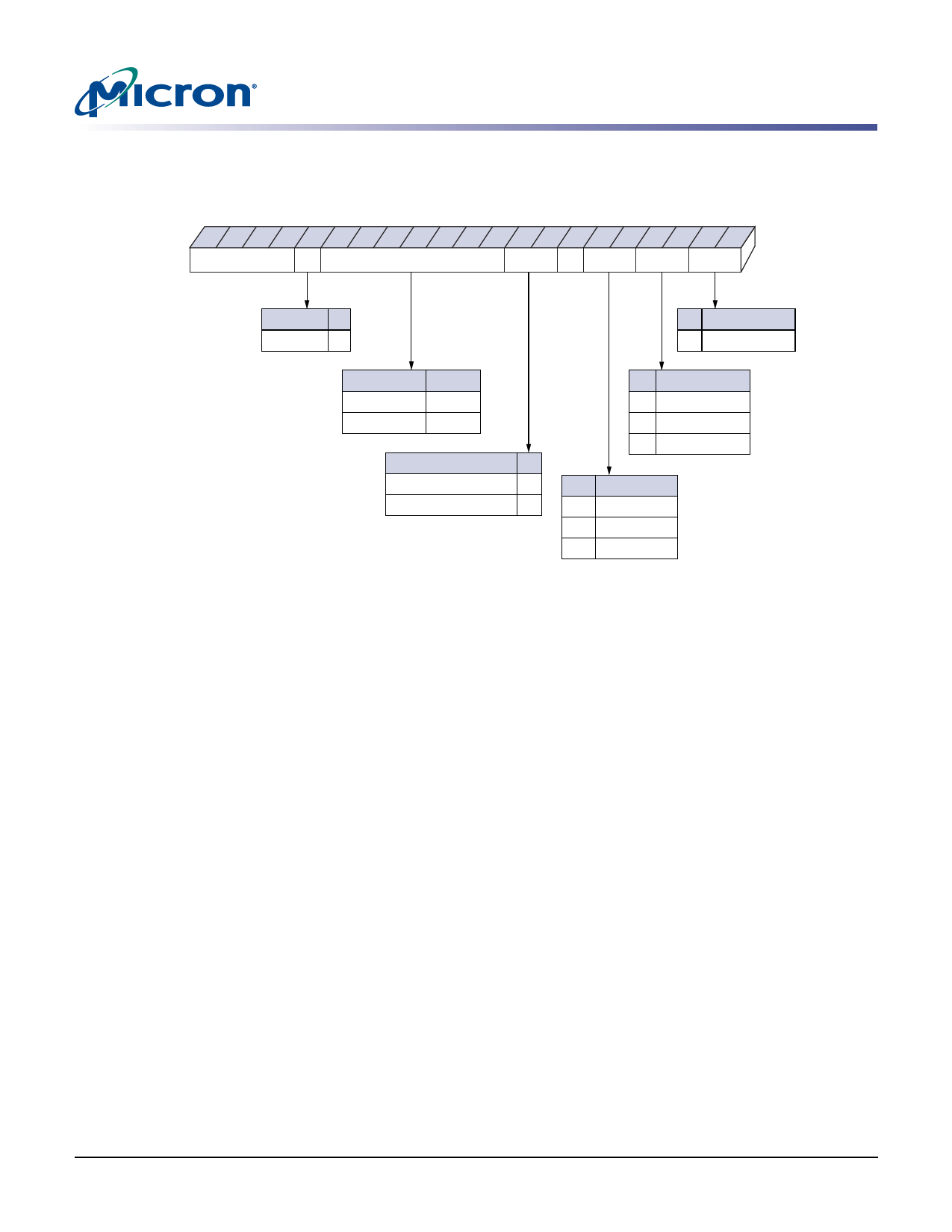
Figure 1: 256Mb Mobile DDR Part Numbering
Example Part Number: MT46H16M 16LFXX-75IT :A
Micron DDR MT46
VDD/
VDDQ
Mobile Configuration
Package – Speed Temp Revision
VDD/VDDQ
1.8V/1.8V H
Configuration
16 Meg x 16 16M16LF
8 Meg x 32
8M32LF
Package
60-Ball VFBGA (lead-free) BF
90-Ball VFBGA (lead-free) B5
Revision
:A First Generation
Operating Temp
Commercial
IT Industrial
Speed Grade
-6 tCK = 6.0ns
-75 tCK = 7.5ns
-10 tCK = 9.6ns
FBGA Part Marking Decoder
Due to space limitations, FBGA-packaged components have an abbreviated part
marking that is different from the part number. For a quick conversion of an FBGA code,
see the FBGA part marking decoder at www.micron.com/decoder.
General Description
The 256Mb Mobile DDR SDRAM is a high-speed CMOS, dynamic random-access
memory containing 268,435,456 bits. It is internally configured as a quad-bank DRAM.
On the x16 device, each of the 67,108,864-bit banks is organized as 8,192 rows by 512
columns by 16 bits. On the x32 device, each of the 67,108,864-bit banks is organized as
4,096 rows by 512 columns by 32 bits.
The 256Mb Mobile DDR SDRAM uses a double data rate architecture to achieve high-
speed operation. The double data rate architecture is essentially a 2n-prefetch architec-
ture with an interface designed to transfer two data words per clock cycle at the I/O
balls. A single read or write access for the 256Mb Mobile DDR SDRAM effectively
consists of a single 2n-bit-wide, one-clock-cycle data transfer at the internal DRAM core
and two corresponding n-bit-wide, one-half-clock-cycle data transfers at the I/O balls.
A bidirectional data strobe (DQS) is transmitted externally, along with data, for use in
data capture at the receiver. DQS is a strobe transmitted by the Mobile DDR SDRAM
during READs and by the memory controller during WRITEs. DQS is edge-aligned with
data for READs and center-aligned with data for WRITEs. The x16 offering has two data
strobes: one for the lower byte and one for the upper byte. The x32 offering has four data
strobes, one per byte.
PDF: 09005aef82091978 / Source: 09005aef8209195b
MT46H16M16LF__2.fm - Rev. H 6/08 EN
5
Micron Technology, Inc., reserves the right to change products or specifications without notice.
©2005 Micron Technology, Inc. All rights reserved.
Share Link: 