MT48H16M16LFB5-8G 데이터 시트보기 (PDF) - Micron Technology
부품명
상세내역
제조사
MT48H16M16LFB5-8G Datasheet PDF : 71 Pages
| |||
256Mb: 16 Meg x 16, 8 Meg x 32 Mobile SDRAM
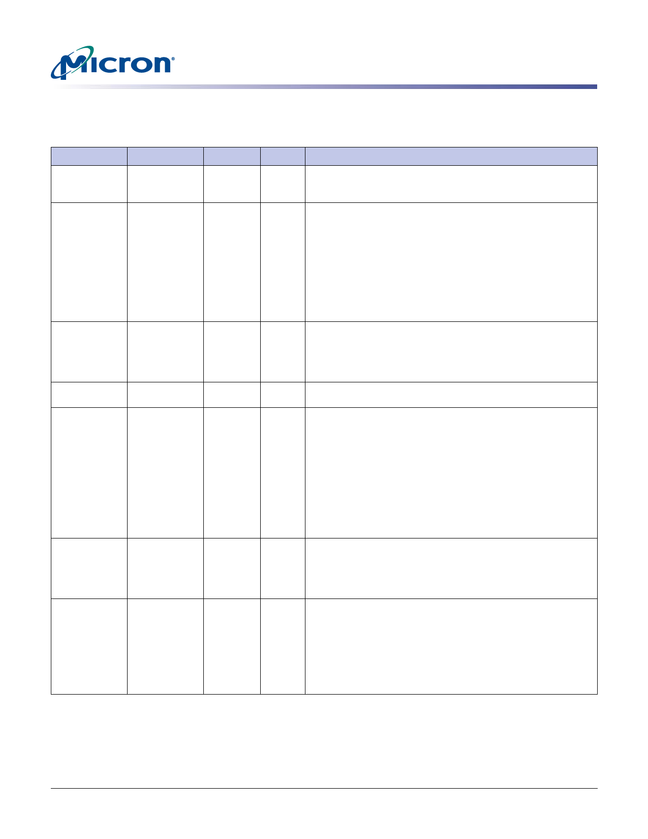
Ball Descriptions
Ball Descriptions
Table 3: VFBGA Ball Descriptions
54-Ball VFBGA 90-Ball VFBGA Symbol
F2
J1
CLK
F3
J2
CKE
G9
J8
CS#
F7, F8, F9
F1, E8
K7, J9, K8
K9, K1, F8, F2
CAS#,
RAS#, WE#
UDQM
LDQM,
DQM0–
DQM3
G7, G8
J7, H8
BA0, BA1
H7, H8, J8, J7,
J3, J2, H3, H2,
H1, G3, H9, G2,
G1
G8, G9, F7, F3,
G1, G2, G3, H1,
H2, J3, G7, H9
A0–A12
Type
Input
Input
Input
Input
Input
Input
Input
Description
Clock: CLK is driven by the system clock. All SDRAM input signals
are sampled on the positive edge of CLK. CLK also increments
the internal burst counter and controls the output registers.
Clock enable: CKE activates (HIGH) and deactivates (LOW) the
CLK signal. Deactivating the clock provides precharge power-
down and SELF REFRESH operation (all banks idle), ACTIVE
power-down (row active in any bank), Deep power-down (all
banks idle), or CLOCK SUSPEND operation (burst/access in
progress). CKE is synchronous except after the device enters
power-down and self refresh modes, where CKE becomes
asynchronous until after exiting the same mode. The input
buffers, including CLK, are disabled during power-down and self
refresh modes, providing low standby power.
Chip select: CS# enables (registered LOW) and disables
(registered HIGH) the command decoder. All commands are
masked when CS# is registered HIGH. CS# provides for external
bank selection on systems with multiple banks. CS# is considered
part of the command code.
Command inputs: RAS#, CAS#, and WE# (along with CS#) define
the command being entered.
Input/output mask: DQM is sampled HIGH and is an input mask
signal for write accesses and an output enable signal for read
accesses. Input data is masked during a WRITE cycle. The output
buffers are placed in a High-Z state (two-clock latency) during a
READ cycle. For the x16, LDQM corresponds to DQ0–DQ7 and
UDQM corresponds to DQ8–DQ16. For the x32, DQM0
corresponds to DQ0–DQ7, DQM1 corresponds to DQ8–DQ15,
DQM2 corresponds to DQ16–DQ23, and DQM3 corresponds to
DQ24–DQ31. DQM0–DQM3 (or LDQM and UDQM if x16) are
considered same state when referenced as DQM. DQM loading is
designed to match that of DQ balls.
Bank address input(s): BA0 and BA1 define to which bank the
ACTIVE, READ, WRITE, or PRECHARGE command is being
applied. These balls also provide the op-code during a LOAD
MODE REGISTER (LMR) command. BA0 and BA1 become “Don’t
Care” when registering an ALL BANK PRECHARGE (A10 HIGH).
Address inputs: A0–A12 are sampled during the ACTIVE
command (row-address A0–A12) and READ/WRITE command
(column-address A0–A8 [x32]; column-address A0–A8 [x16]; with
A10 defining auto precharge) to select one location out of the
memory array in the respective bank. A10 is sampled during a
PRECHARGE command to determine if all banks are to be
precharged (A10 HIGH) or bank selected by BA0, BA1. The
address inputs also provide the op-code during a LMR command.
PDF:09005aef8219eeeb/Source: 09005aef8219eedd
MT48H16M16LF_2.fm - Rev F 4/07 EN
10
Micron Technology, Inc., reserves the right to change products or specifications without notice.
©2006 Micron Technology, Inc. All rights reserved.
Share Link: 