RF3159 데이터 시트보기 (PDF) - RF Micro Devices
부품명
상세내역
제조사
RF3159 Datasheet PDF : 26 Pages
| |||
RF3159
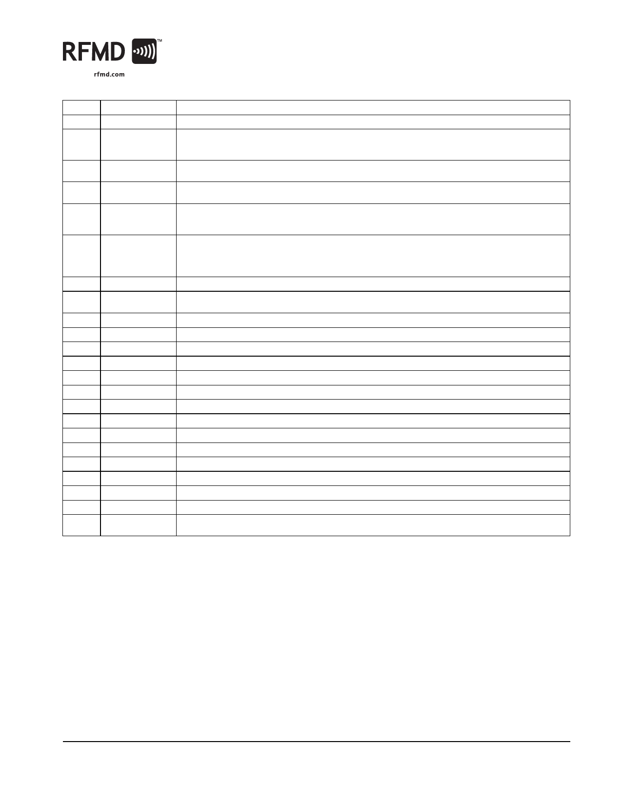
Pin
Function Description
1
HB_RFIN RF input to the high-band PA. It is DC-blocked within the part.
2
BAND_SEL Digital input enables either the low band or high band amplifier die within the module. A logic low selects Low
Band (GSM850/EGSM900), a low logic high selects High Band (DCS1800/PCS1900). This pin is a high imped-
ance CMOS input with no pull-up or pull-down resistors.
3
TX_EN
Digital input enables or disables the internal circuitry. When disabled, the module is in the OFF state, and
draws virtually zero current. This pin is a high impedance CMOS input with no pull-up or pull-down resistors.
4
VBATT
Main DC power supply for all circuitry in the RF3159. Traces to this pin will have high current pulses during
operation so proper decoupling and routing should be observed.
5
VMODE
Digital input which internally adjusts settings to optimize amplifier performance for saturated or linear mode. A
logic low selects saturated mode for GMSK modulation. A logic high selects linear mode for 8PSK modulation.
This pin is a high impedance CMOS input with no pull-up or pull-down resistors.
6
VRAMP
In GMSK mode, the voltage on this pin controls the output power by varying the regulated collector voltage of
the amplifiers. In EDGE mode, this pin has no effect. An internal 300kHz filter reduces switching ORFS result-
ing from transitions between DAC steps. Most systems will have no need for external VRAMP filtering. This pin
provides an impedance of approximately 60kΩ.
7
LB_RFIN
RF input to the low-band PA. It is DC-blocked within the part.
8
VBIAS
Bias selection logic pin. A logic low selects a low bias (current saving mode) which will only meet linearity per-
formance at low power levels. A logic high allows linear performance up to the highest supported output power.
9
GND
Ground.
10
GND
Ground.
11
GND
Ground.
12
LB_RFOUT RF output from the low-band PA. It is DC-blocked within the part.
13
GND
Ground.
14
GND
Ground.
15
GND
Ground.
16
GND
Ground.
17
GND
Ground.
18
HB_RFOUT RF output from the high-band PA. It is DC-blocked within the part.
19
GND
Ground.
20
GND
Ground.
21
GND
Ground.
22
GND
Ground.
23
GND
Main ground pad in center of part. This pad should be tied to the main ground plane with as little loss as pos-
sible for optimum linearity.
Rev A0 DS070102
7628 Thorndike Road, Greensboro, NC 27409-9421 · For sales or technical
support, contact RFMD at (+1) 336-678-5570 or sales-support@rfmd.com.
11 of 26
Share Link: 