RT8855 데이터 시트보기 (PDF) - Richtek Technology
부품명
상세내역
제조사
RT8855 Datasheet PDF : 18 Pages
| |||
RT8855
Table 3. SVI Send Byte-Address and Data Phase
Description / Example
bits Description
Address Phase
6 : 4 Always 110b
3
Not Applicable, ignored.
2
Not Applicable, ignored.
CORE Section. (Note)
1
If set then the following data byte contains the
VID code for CORE Section.
NB Section. (Note)
0
If set then the following data byte contains the
VID code for NB Section.
Data Phase
7
PSI_L Flag (Active Low). When asserted, the
VR is allowed to enter Power-Saving Mode.
6 : 0 VID Code.
Note : Assertion in both bit 1 and 0 will address the VID
code to both CORE and NB simultaneously.
Example :
SVI Address
Bits [6 : 0]
1100_000
1100_001
1100_110
1100_100
1100_010
1100_111
Description
Should be ignored.
Set VID on VDDNB.
Set VID on VDD0 and VDD1.
Set VID on VDD1.
Set VID on VDD0 or VDD (uniplane).
Set VID on VDDNB, VDD0 and
VDD1.
PWROK De-assertion
PWROK stays low after EN signal is asserted, and the
controller regulates all the planes according to the Pre-
PWROK Metal VID.
PGOOD is de-asserted as long as Pre-PWROK Metal VID
voltage is out of the initial voltage specifications.
V_FIX Mode Function
Anytime the pin VID0/VFIXEN is pulled high, the controller
enters V-FIX mode. When in V_FIX mode, both VCORE
and NB section voltages are governed by the information
shown in Table 4. Regardless of the state of PWROK, the
device will work in SVI mode. SVC and SVD are considered
as static VID and the output voltage will be changed
according to their status. Dynamic SVC/SVD-change
management is provided in this condition. V_FIX mode is
intended for system debug only.
DS8855-01 April 2011
Table 4. V_FIX Mode and Pre-PWROK Metal VID
Output Voltage (V)
SVC
SVD Pre-PWROK
V_FIX Mode
Metal VID
0
0
1.1V
1.4V
0
1
1.0V
1.2V
1
0
0.9V
1.0V
1
1
0.8V
0.8V
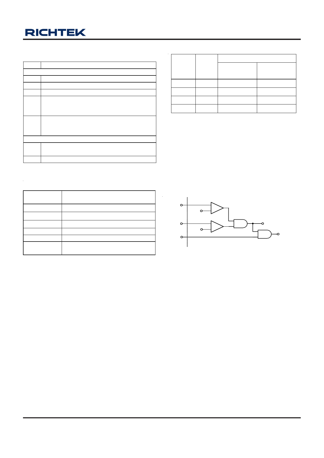
Power Ready Detection
During start-up, RT8855 will detect VCC12, VCC5 and
EN signal. Figure 2 shows the power ready detection
circuit. When VCC12 > 9.6V and VCC5 > 4.6V, POR
(Power On Reset) will go high. POR is the internal signal
to indicate all input powers are ready to let RT8855 and
the companioned MOSFET drivers to work properly. When
POR = L, RT8855 will turn off both high side and low side
MOSFETs.
VCC12
9.6V
CMP
+
-
VCC5
EN
4.6V
CMP
+
-
POR
Chip Enable
Figure 2. Circuit for Power Ready Detection
Power-Up Sequencing
Figure 3 and 4 are the power-up sequencing diagram of
RT8855. Once power_on_reset is valid (POR = H), on the
rising edge of the EN signal, the RT8855 detects the VID1
pin and determine to operate either in SVI or PVI mode.
Figure3 shows the PVI-mode power sequence, the
controller stays in T1 state waiting for valid parallel VID
code sent by CPU. After receiving valid parallel VID code,
VCORE continues ramping up to the specified voltage
according to the VID code in T2 state. Figure 4 shows the
SVI-mode power sequence, the controller samples the
two serial VID pins, SVC and SVD. Then, the controller
stores this value as the boot VID that is the so-called
“Pre-PWROK Metal VID” in T1 state. After the processor
starts with boot VID voltages, PWROK is asserted and
the processor initializes the serial VID interface in T2 state.
The processor uses the serial VID interface to issue VID
commands to move the power planes from the boot VID
values to the dual power planes in T3 state.
www.richtek.com
11
Share Link: 