ST8012 데이터 시트보기 (PDF) - Sitronix Technology Co., Ltd.
부품명
상세내역
제조사
ST8012 Datasheet PDF : 47 Pages
| |||
ST8012
5. FUNCTIONAL DESCRIPTION
5.1 Pin Functions
(Segment mode)
SYMBOL
FUNCTION
VDD
Logic system power supply pin, connected to +2.5 to +5.5 V.
VSS
Ground pin, connected to 0 V.
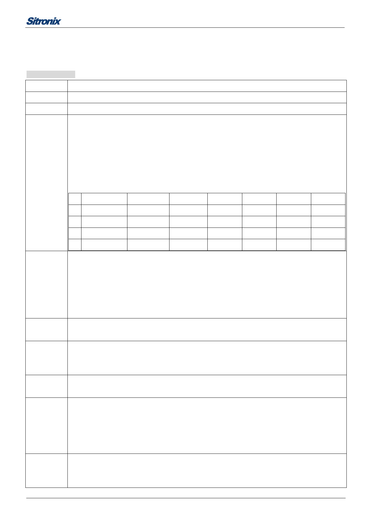
This is a multi-level power supply for the liquid crystal drive. The voltage Supply applied is determined
by the liquid crystal cell, and is changed through the use of a resistive voltage divided or through
changing the impedance using an op. amp. Voltage levels are determined based on VSS, and must
maintain the relative magnitudes shown below.
V0 V1
V2 V3
V4
V0 ≧V1 ≧V2 ≧V3 ≧V4 ≧Vss
When the power supply turns ON, the internal power supply circuits produce the V1to V4voltages shown below.
The voltage settings are selected using the LCD bias set command.
1/120 Duty
1/112 Duty
1/96Duty 1/80Duty 1/64Duty 1/48 Duty 1/30 Duty
V4 1/11*V0 ,1/9*V0 1/11*V0, 1/9*V0 1/10*V0, 1/8*V0 1/9*V0, 1/7*V0 1/9*V0, 1/7*V0 1/7*V0, 1/5*V0 1/6*V0, 1/5*V0
V3 2/11*V0,1/9*V0 2/11*V0, 2/9*V0 2/10*V0, 2/8*V0 2/9*V0, 2/7*V0 2/9*V0, 2/7*V0 2/7*V0, 2/5*V0 2/6*V0, 2/5*V0
V2 9/11*V0, 7/9*V0 9/11*V0, 7/9*V0 8/10*V0, 6/8*V0 7/9*V0, 5/7*V0 7/9*V0, 5/7*V0 5/7*V0, 3/5*V0 4/6*V0, 3/5*V0
V1 10/11*V0,8/9*V0 10/11*V0,8/9*V0 9/10*V0, 7/8*V0 8/9*V0, 6/7*V0 8/9*V0, 6/7*V0 6/7*V0, 4/5*V0 5/6*V0, 4/5*V0
Input pins for display data
In 4-bit parallel input mode, input data into the 4 pins, DI3-DI0.
DI3-DI0
In serial input mode, input data into the 1 pin,DI0.
Connect DI3-DI1 to VSS .
Refer to "RELATIONSHIP BETWEEN THE DISPLAY DATA AND LCD DRIVE OUTPUT
PINS" in Functional Operations.
XCK
Clock input pin for taking display data
* Data is read at the falling edge of the clock pulse.
System Reset pin .When low level active.
XRST If not used the hardware reset, this pin must pull height.
The XRST L PULSE timing min value is 200us and max value is 0.5s
Latch pulse input pin for display data
LP
Data is latched at the falling edge of the clock pulse.
Input pin for selecting the reading direction of display data
When set to VSS level "L", data is read sequentially from COMSEG119 to COMSEG0.
L/R
When set to VDD level "H", data is read sequentially from COMSEG0 to COMSEG119.
Refer to "RELATIONSHIP BETWEEN THE DISPLAY DATA AND LCD DRIVE OUTPUT
PINS" in Functional Operations.
Control input pin for output of non-select level
XDISPOFF The input signal is level-shifted from logic voltage level to LCD drive voltage level, and controls the
LCD drive circuit.
V1.6
7/47
2004/09/08
Share Link: 