TEA1507 데이터 시트보기 (PDF) - Philips Electronics
부품명
상세내역
제조사
TEA1507 Datasheet PDF : 20 Pages
| |||
Philips Semiconductors
GreenChip™II SMPS control IC
Preliminary specification
TEA1507
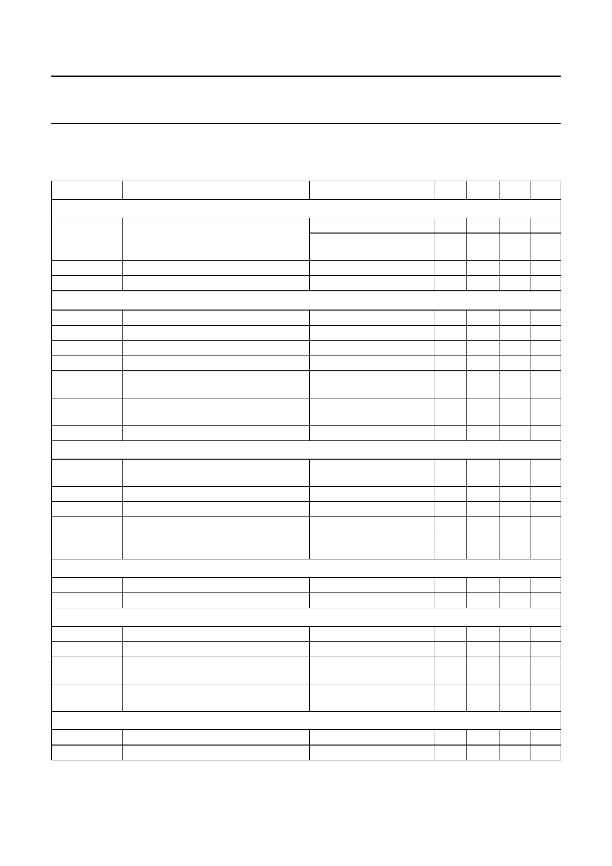
CHARACTERISTICS
Tamb = 25 °C; VCC = 15 V; all voltages are measured with respect to ground (pin 2); currents are positive when flowing
into the IC; unless otherwise specified.
SYMBOL
PARAMETER
CONDITIONS
MIN. TYP. MAX. UNIT
Start-up current source (pin 8)
Ii(DRAIN)
BVDSS
M-level
supply current drawn from drain pin
VCC = 0 V; VDRAIN > 100 V 1.0 1.2 1.4 mA
with auxiliary supply;
VDRAIN > 100 V
−
100 300 µA
breakdown voltage
650 −
−
V
mains-dependent operation-enabling level
60 −
100 V
VCC management (pin 1)
VCC(start)
VCC(UVLO)
VCC(hys)
Ii(VCC)H
Ii(VCC)L
IVCC(restart)
ICC(operate)
start-up voltage on VCC
under voltage lock-out on VCC
hysteresis voltage on VCC
pin VCC charging current
pin VCC charging current
pin VCC restart current
supply current under normal operation
10.3
8.1
VCC(start) − VCC(UVLO)
VDRAIN > 100 V; VCC < 3V
VDRAIN > 100 V;
3 V < VCC < VCC(UVLO)
VDRAIN > 100 V;
VCC(UVLO) < VCC < VCC(start)
no load on pin DRIVER
2.0
−1.2
−1.2
−650
1.1
11 11.7 V
8.7 9.3 V
2.3 2.6 V
−1 −0.8 mA
−0.75 −0.45 mA
−550 −450 µA
1.3 1.5 mA
Demagnetization management (pin 4)
VDEM
demagnetization comparator threshold
voltage on pin DEM
IDEM
pin DEM current
Vclamp(DEM)(neg) negative clamp voltage on pin DEM
Vclamp(DEM)(pos) positive clamp voltage on pin DEM
tsuppr
suppression of transformer ringing at start
of secondary stroke
VDEM = 50 mV
at IDEM = −150 µA
at IDEM = 250 µA
50 100 150 mV
−50(1) −
0
nA
−0.5 −0.25 −0.05 V
0.5 0.7 0.9 V
1.1 1.5 1.9 µs
Pulse width modulator
ton(min)
ton(max)
minimum on-time
maximum on-time
latched
−
tleb
−
ns
40 50 60 µs
Oscillator
foscL
foscH
Vvco(start)
oscillator low frequency (fixed frequency) VCTRL > 1.5 V
oscillator high frequency (fixed frequency) VCTRL < 1 V
peak voltage at pin Isense, where
frequency reduction starts
see Fig.6
5
6.5 8
kHz
145 175 205 kHz
−
75 −
mV
Vvco(max)
peak voltage at pin Isense, where the
frequency is equal to foscL
−
50 −
mV
Duty cycle control (pin 3)
VCTRL(min)
VCTRL(max)
min. voltage on CTRL (max. duty cycle)
max. voltage on CTRL (min. duty cycle)
−
1.0 −
V
−
1.5 −
V
2000 Dec 05
11
Share Link: 