CDP68HC68T1(1997) 데이터 시트보기 (PDF) - Intersil
부품명
상세내역
제조사
CDP68HC68T1 Datasheet PDF : 24 Pages
| |||
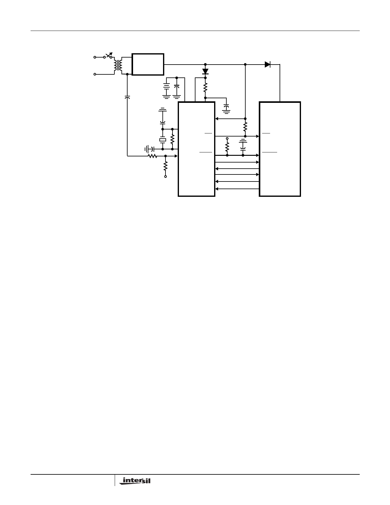
System Diagrams (Continued)
CDP68HC68T1
AC
LINE
BRIDGE
GENERATOR
VBATT
VDD
POR
VSYS
VDD
INT
VDD
CDP68HC68T1
LINE CPUR
CLK OUT
CE
MISO
MOSI
SCK
VDD
IRQ
CDP68HC05C8B
RESET
OSC 1
PORT (e.g., PCO)
MISO
MOSI
SCK
NOTE: Example of a system in which the power is controlled by an external source. The LINE input pin can sense when the switch opens by use
of the POWER-SENSE INTERRUPT. The CDP68HC68T1 crystal drives the clock input to the CPU using the CLK OUT pin. On power down when
VSYS < VBATT + 0.7V. VBATT will power the CDP68HC68T1. A threshold detect activates a P-Channel switch, connecting VBATT to VDD. VBATT
always supplies power to the oscillator, keeping voltage frequency variation to a minimum.
FIGURE 17. EXTERNALLY CONTROLLED POWER SYSTEM DIAGRAM
A Procedure for Power-Down Operation might consist of the following:
1. Set power sense operation by writing bit 5 high in the Interrupt Control Register.
2. When an interrupt occurs, the CPU reads the Status Register to determine the interrupt source.
3. Sensing a power failure, the CPU does the necessary housekeeping to prepare for shutdown.
4. The CPU reads the Status Register again after several milliseconds to determine validity of power failure.
5. The CPU sets power-down bit 6 and disables all interrupts in the Interrupt Control Register when power down is verified. This
causes the CPU reset and clock out to be held low and disconnects the serial interface.
6. When power returns and VSYS rises above VBATT, power down is terminated. The CPU reset is released and serial communi-
cation is established.
18
Share Link: 