HSP50215 데이터 시트보기 (PDF) - Intersil
부품명
상세내역
제조사
HSP50215 Datasheet PDF : 21 Pages
| |||
HSP50215
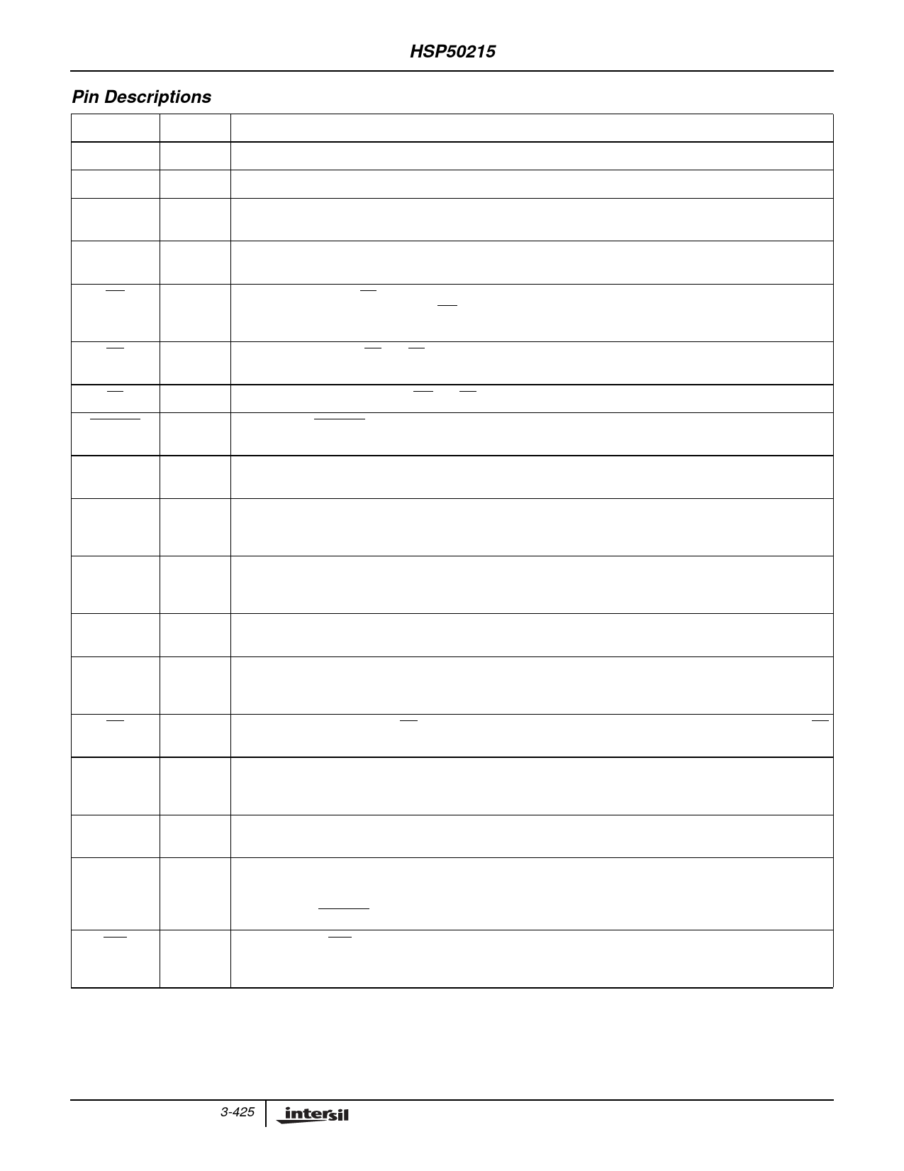
Pin Descriptions
NAME
TYPE
VCC
-
GND
-
C(15:0)
I/O
A(9:0)
I
WR
I
RD
I
CE
I
FIFORDY
O
REFCLK
I
CAS(15:0)
I
CASZ
I
OUT(15:0)
O
OFM
I
OE
I
SYNCIN
I
SYNCOUT
O
SAMPCLK
O
RST
I
DESCRIPTION
+5V Power supply input.
Power supply ground input.
µP Bidirectional Data bus. The C(15:0) bus is used for loading the configuration data and sample vectors for mod-
ulation. C15 is the MSB.
µP Address Bus. The A(9:0) bus is used for addressing the proper registers for loading the configuration data and
sample vectors for modulation. A9 is the MSB.
µP Write Strobe. When CE is asserted, data on the C(15:0) data bus is loaded into the address location found on
the A(9:0) bus on the rising edge of the WR signal. In some cases, there is an internal synchronization to the master
clock that must be completed before the next data is written. See the µP interface section for more information.
µP Read Control. When RD and CE are low, the data found in the address location defined by A(9:0) is routed to
the C(15:0) µP data bus on the next rising edge of REFCLK.
µP Chip Enable. Used to gate the WR and RD µP interface control signals.
FIFO Ready. A FIFORDY assertion indicates that the I and Q FIFOs have reached the programmed FIFO depth and
more samples are required to maintain that FIFO depth.
Reference Clock. REFCLK is the master clock for the DUC. All timing is relative to the REFCLK rising edge. The
frequency of the reference clock is denoted fCLK, and is the rate at which data is output from the part.
Cascade Input Bus. This input bus is used to cascade multiple parts by routing the digital modulated signal from
one DUC into the output summer of a second DUC. CAS(15:0) is 2’s complement format and is sampled on the
rising edge of REFCLK. CAS15 is the MSB.
Cascade Input Bus Zero. When CASZ is asserted (pulled high), the part places zeroes on the CAS(15:0) data path.
CASZ is asynchronous (not registered) to REFCLK and should not be changed on the fly. When unused, pull high
with a pull up resistor (~22kΩ).
Output Data Bus. OUT(15:0) contains the digital modulated DUC output samples and is updated on the rising edge
of the REFCLK. OUT15 is the MSB.
Output Data Bus Format. When OFM is asserted (pulled high), the output bus format is 2’s complement. When not
asserted, the output format is offset binary. The OFM input is asynchronous (not registered) to REFCLK and should
not be changed on the fly.
Output Data Bus Enable. When OE is asserted (dropped low), the output data bus OUT(15:0) is enabled. When OE
is not asserted (pulled high), the output data bus OUT(15:0) is placed in the high impedance state.
Sync Input. The SYNCIN input is used to synchronize the processing of multiple parts. The SYNCOUT of one part
acts as a master and is connected to the SYNCIN of all of the DUC’s that are to by synchronized. The DUC can be
programmed so that either rising or falling edge of this signal initiates the processing.
Sync Output. The SYNCOUT output is used to synchronize the processing of multiple parts. The SYNCOUT of one
part acts as a master, and is connected to the SYNCIN of all of the DUC’s that are to be synchronized.
Sample Clock. This clock is provided to the data source to indicate when data is being transferred from the FIFO to
the shaping filter. The SAMPCLK output is generated by the sample rate NCO when the digital filter takes a new
sample. It has approximately 50% duty cycle. The sample is taken on the high-to-low transition. SAMPCLK may be
used instead of FIFORDY.
Reset. When the RST input is asserted (dropped low), the DUC is reset and all processing halts. The DUC may
also be reset on µP command. Processing remains halted until a sync is generated either by µP command or
assertion of SYNCIN. See the Reset section details of the specific functions halted by this control signal.
3-425
Share Link: 