HSP50215 데이터 시트보기 (PDF) - Intersil
부품명
상세내역
제조사
HSP50215 Datasheet PDF : 21 Pages
| |||
HSP50215
of a quadrature NCO to produce a zero I.F. FM signal. These
FM modulated quadrature samples are then up sampled in
the interpolation filter to the output sample rate. The
baseband modulated signal is then upconverted to the
carrier frequency by the carrier NCO and mixers. The output
is then summed with the cascade input signal, saturated,
and formatted for output.
SHAPING
FM
INTERPOLATION
I
FILTER
MODULATOR
FILTER
FIGURE 6. FM WITH PULSE SHAPING
In Mode 10, the amplitude out of the shaping filter needs to
be limited in order to prevent frequency excursions that
cannot be filtered out in the interpolation filter. The quality of
the FM signal is affected by the amplitude slew rate out of
the shaping filter. As a rule of thumb, limiting this slew rate to
less than 1/8 the sample rate will minimize this distortion.
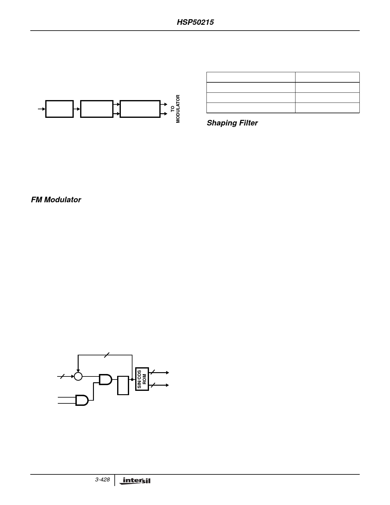
FM Modulator
The FM modulator provides for frequency modulation of the
carrier center frequency by the PUC input data. The FM
modulator is driven either directly by the PUC I input (Mode
1) or by the output of the FIR shaping filter (Mode 2). The
input data to the FM Modulator, is defined as dφ(n)/dt, where
φ(nT) is the phase of a theoretical sinusoid described by:
s(n) = A (cos[φ(nT) ]+ j sin [φ(nT)]); A ≈ 1 in Modulator (EQ. 1)
Figure 7 illustrates the conceptual design of the FM modulator.
The input to the FM modulator, dφ(n)/dt, is integrated via the
carrier NCO accumulator. The NCO accumulator output
represents phase and is used to address a SIN/COS generator,
synthesizing a sinusoid of the form described in Equation 1.
The phase accumulator feedback of the NCO is 16 bits and
sixteen bits of the phase word are routed to the SIN/COS
generator. Sixteen bits of resolution are provided on the Sine
and Cosine outputs.
16
dφ(nT)/dt
∑
EnNCO
MODE
1 OR 2
16
φ(nT)
16 COS[φ(nT)]
R
16 SIN[φ(nT)]
E
>G
FIGURE 7. FM MODULATOR BLOCK DIAGRAM
The transfer function of the FM modulator is defined by the
change in degrees per sample value, dφ(nT)/dt, where
dφ(nT)/dt is a 16-bit, twos complement, fractionally notated
frequency control word with a range from -FSAMP/2 to
+FSAMP/2. FSAMP is defined as the sample rate into FM
modulator. The maximum phase step that can occur in one
clock is ±180 degrees. Table 1 provides the change in phase
weighting of the input bits.
TABLE 1. FM MODULATOR TRANSFER FUNCTION
dφ(nT)/dt
DEGREES/SAMPLE
1000 0000 0000 0000
-180
0000 0000 0000 0000
0
0111 1111 1111 1111
~+180
Shaping Filter
The shaping filter provides the necessary pulse shaping
required on the input data to implement various quadrature
ASK and shaped FM modulation formats. Two identical
shaping filters (one each for the I and Q channels) are
provided. The filters can implement a 4-16 input sample
span impulse response using up to 256 taps with 16 bits of
resolution in the coefficients.
The range of valid digital values for the coefficients is from
8001 to 7FFF. The value 8000 is not allowed. The coefficient
format is 2’s complement. The span of the Impulse response
of the polyphase filter can be from 4-16 samples. The
desired sample span value minus one is programmed into
the Data Samples (DS) field in Control Word 19, bits 2-5.
The filter has a programmable interpolation rate (IP) of 4, 8,
or 16. This interpolation rate is programmed by Control
Address 19, bits 0 and 1. Thus, the required number of
coefficients (or filter span) becomes
# Coefficients = (DS)(IP)
(EQ. 2)
with 256 being the maximum number of coefficients.
Note that
REFCLK > (DS)(IP)(fS)
(EQ. 3)
where fS is the input sample rate of the shaping filter. For a
16 input sample impulse response span, the total impulse
response is 64, 128 or 256 filter taps for interpolation rates of
4, 8 or 16, respectively. The filter structure precludes
coefficient re-use for symmetric filters, so both asymmetric
and symmetric filters have up to 256 taps available and are
loaded in identical manner.
The maximum input sample rate is:
fS = fCLK ⁄ [(IP)(DS) ]
(EQ. 4)
where fCLK is the frequency of the reference clock, IP is the
shaping filter interpolate rate; and DS is the number of data
samples in the filter span. For example, if fCLK = 52MHz, the
filter span is 16 samples, and the interpolation rate is 16,
then the maximum input sample rate, fS is 52/256 = 203kHz.
Table 2 shows several examples of calculations for FIR input
sample rates based on master reference clock rate, number
of data samples, and interpolation rate.
3-428
Share Link: 