DS28E04-100 데이터 시트보기 (PDF) - Dallas Semiconductor -> Maxim Integrated
부품명
상세내역
제조사
DS28E04-100 Datasheet PDF : 36 Pages
| |||
DS28E04-100: 4096-Bit 1-Wire Addressable EEPROM with PIO
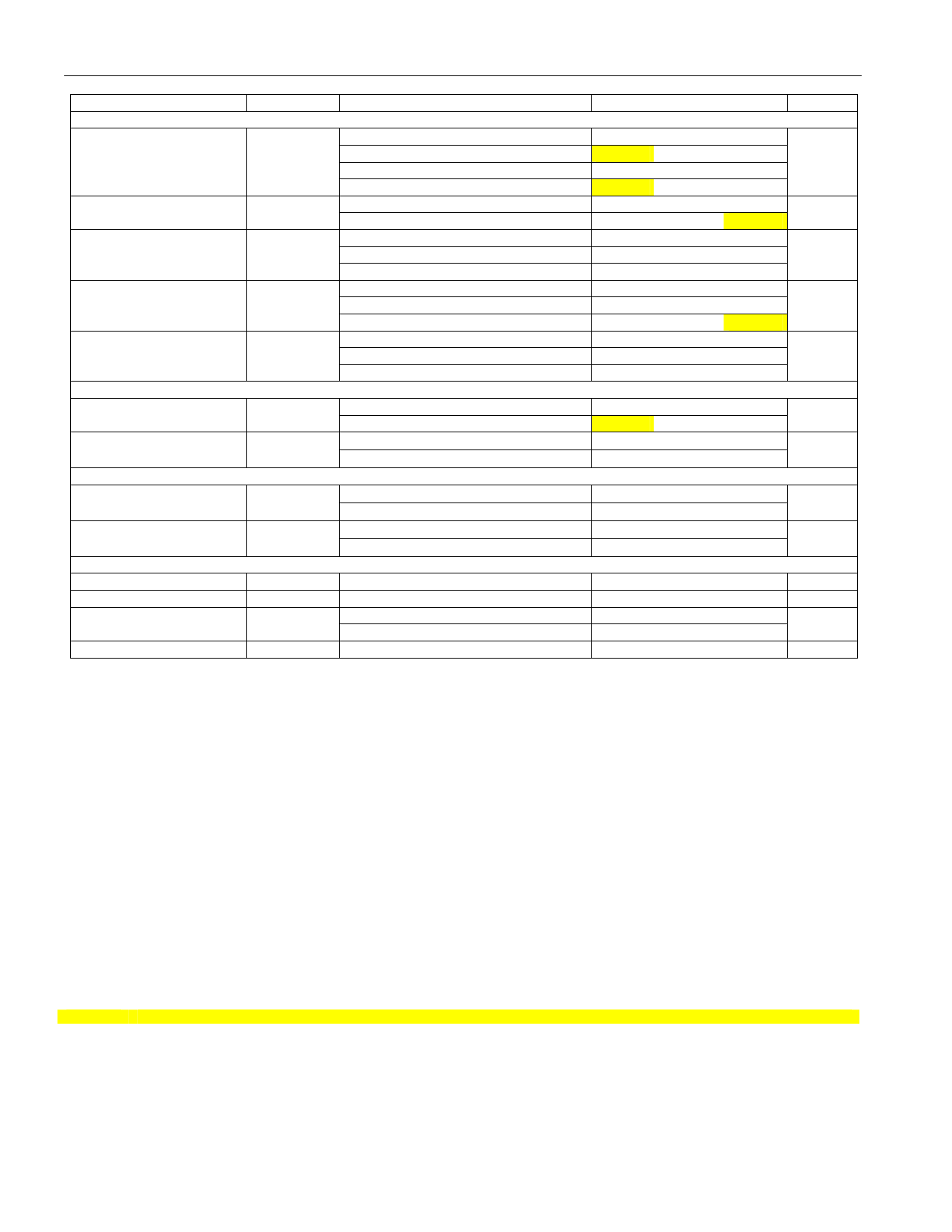
PARAMETER
SYMBOL
CONDITIONS
IO PIN, 1-Wire RESET, PRESENCE DETECT CYCLE
Reset Low Time (Note 1)
tRSTL
Standard speed, VPUP > 4.5V
Standard speed (Note 17)
Overdrive speed, VPUP > 4.5V
Overdrive speed (Note 17)
Presence-Detect High
Time
tPDH
Standard speed
Overdrive speed (Note 17)
Presence-Detect Fall Time
(Notes 3, 18)
tFPD
Standard speed, VPUP > 4.5V
Standard speed
Overdrive speed
Presence-Detect Low
Time
Standard speed
tPDL
Overdrive speed, VPUP > 4.5V
Overdrive speed (Note 17)
Presence-Detect Sample
Time (Note 1)
Standard speed, VPUP > 4.5V
tMSP
Standard speed
Overdrive speed
IO PIN, 1-Wire WRITE
Write-0 Low Time (Note 1)
tW0L
Standard speed
Overdrive speed (Note 17)
Write-1 Low Time
(Notes 1, 19)
Standard speed
tW1L
Overdrive speed
IO PIN, 1-Wire READ
Read Low Time
(Notes 1, 20)
tRL
Standard speed
Overdrive speed
Read Sample Time
(Notes 1, 20)
tMSR
Standard speed
Overdrive speed
EEPROM
Programming Current
Programming Time
Write/Erase Cycles
(Endurance)
IPROG
tPROG
NCY
(Note 21)
(Note 22)
At +25°C
At +85°C (worst case)
Data Retention
tDR
At +85°C (worst case)
MIN
480
504
48
53
15
2
1.10
1.1
0
60
8
8
64
67
8.1
60
7
5
1
5
1
tRL + d
tRL + d
200k
50k
10
TYP
MAX
640
640
80
80
60
7
3.75
7.0
1.1
240
24
26
75
75
10
120
16
15 - e
2-e
15 - d
2-d
15
2
1
10
UNITS
µs
µs
µs
µs
µs
µs
µs
µs
µs
mA
ms
¾
years
Note 1:
Note 2:
Note 3:
Note 4:
Note 5:
Note 6:
Note 7:
Note 8:
Note 9:
Note 10:
Note 11:
Note 12:
Note 13:
Note 14:
Note 15:
Note 16:
Note 17:
Note 18:
Note 19:
Note 20:
System requirement.
Maximum instantaneous pulldown current through all pins combined.
Guaranteed by design, simulation only. Not production tested.
This load current is caused by the internal weak pullup, which asserts a logical 1 to address pins that are not connected. The
logical state of the address pins must not change during the execution of ROM function commands during those time slots in
which these bits are relevant.
The I-V characteristic is linear for voltages less than 1V.
Width of the narrowest pulse that trips the activity latch. Back to back pulses that are active for < tPWMIN (max) and that have an
intermediate inactive time < tPWMIN (max) are not guaranteed to be filtered.
The Pulse function requires that VCC power is available; otherwise the command will not be executed.
Maximum allowable pullup resistance is a function of the number of 1-Wire devices in the system and 1-Wire recovery times. The
specified value here applies to systems with only one device and with the minimum 1-Wire recovery times. For more heavily
loaded systems, an active pullup such as that found in the DS2482-x00, DS2480B, or DS2490 may be required.
Capacitance on the data pin could be 800pF when VPUP is first applied. If a 2.2kW resistor is used to pull up the data line, 2.5µs
after VPUP has been applied the parasite capacitance will not affect normal communications.
VTL, VTH, and VHY are a function of the internal supply voltage.
Voltage below which, during a falling edge on IO, a logic 0 is detected.
The voltage on IO needs to be less than or equal to VILMAX whenever the master drives the line low.
Voltage above which, during a rising edge on IO, a logic 1 is detected.
After VTH is crossed during a rising edge on IO, the voltage on IO has to drop by at least VHY to be detected as logic '0'.
Applies to a single DS28E04-100 without VCC supply, attached to a 1-Wire line.
The earliest recognition of a negative edge is possible at tREH after VTH has been previously reached.
Highlighted numbers are NOT in compliance with legacy 1-Wire product standards. See comparison table.
Interval during the negative edge on IO at the beginning of a Presence Detect pulse between the time at which the voltage is
80% of VPUP and the time at which the voltage is 20% of VPUP.
e represents the time required for the pullup circuitry to pull the voltage on IO up from VIL to VTH.
d represents the time required for the pullup circuitry to pull the voltage on IO up from VIL to the input high threshold of the bus
master.
3 of 36
Share Link: 