FSQ110 데이터 시트보기 (PDF) - Fairchild Semiconductor
부품명
상세내역
제조사
FSQ110 Datasheet PDF : 12 Pages
| |||
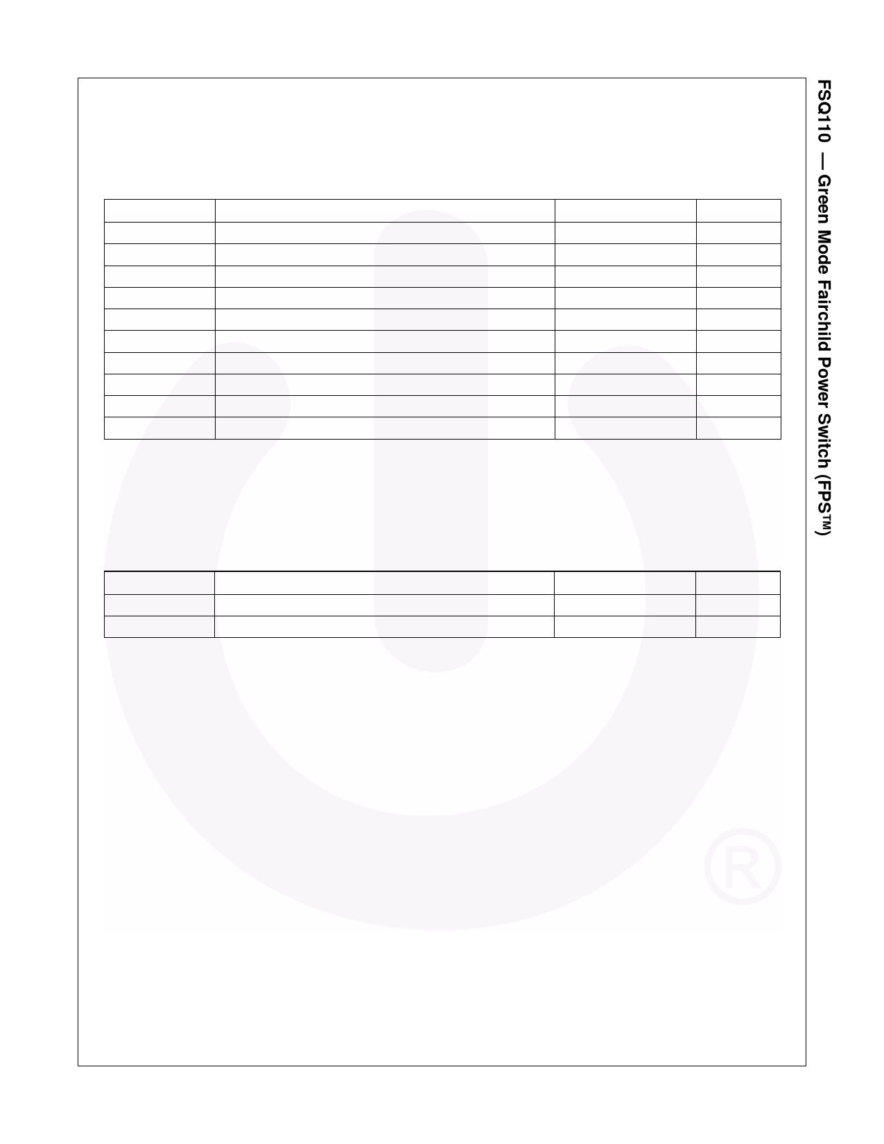
Absolute Maximum Ratings
Stresses exceeding the absolute maximum ratings may damage the device. The device may not function or be
operable above the recommended operating conditions and stressing the parts to these levels is not recommended. In
addition, extended exposure to stresses above the recommended operating conditions may affect device reliability.
The absolute maximum ratings are stress ratings only. TA = 25°C, unless otherwise specified.
Symbol
Characteristic
Value
Unit
VDRAIN
VSTR
IDM
EAS
VCC
VFB
PD
TJ
TA
TSTG
Drain Pin Voltage
Vstr Pin Voltage
Drain Current Pulsed(5)
Single Pulsed Avalanche Energy(6)
Supply Voltage
Feedback Voltage Range
Total Power Dissipation
Operating Junction Temperature
Operating Ambient Temperature
Storage Temperature
650
V
650
V
1.5
A
10
mJ
20
V
-0.3 to VCC
V
1.40
W
Internally limited
°C
-25 to +85
°C
-55 to +150
°C
Notes:
5. Repetitive rating: Pulse width is limited by maximum junction temperature.
6. L = 24mH, starting TJ = 25°C.
Thermal Impedance
TA = 25°C, unless otherwise specified. All items are tested with the standards JESD 51-2 and 51-10 (DIP).
Symbol
θJA
θJC
Parameter
Junction-to-Ambient Thermal Resistance(7)
Junction-to-Case Thermal Resistance(8)
Value
88.84
13.94
Unit
°C/W
°C/W
Notes:
7. Free standing with no heatsink; without copper clad.
(Measurement Condition - Just before junction temperature TJ enters into OTP.)
8. Measured on the DRAIN pin close to plastic interface.
© 2007 Fairchild Semiconductor Corporation
FSQ110 Rev. 1.0.0
4
www.fairchildsemi.com
Share Link: 